Xilinx ML605 User Manual
Page 58
58
ML605 Hardware User Guide
UG534 (v1.8) October 2, 2012
Chapter 1: ML605 Evaluation Board
Mode, Osc Enable, Boot EEPROM Select, and Addr Select DIP Switch S2
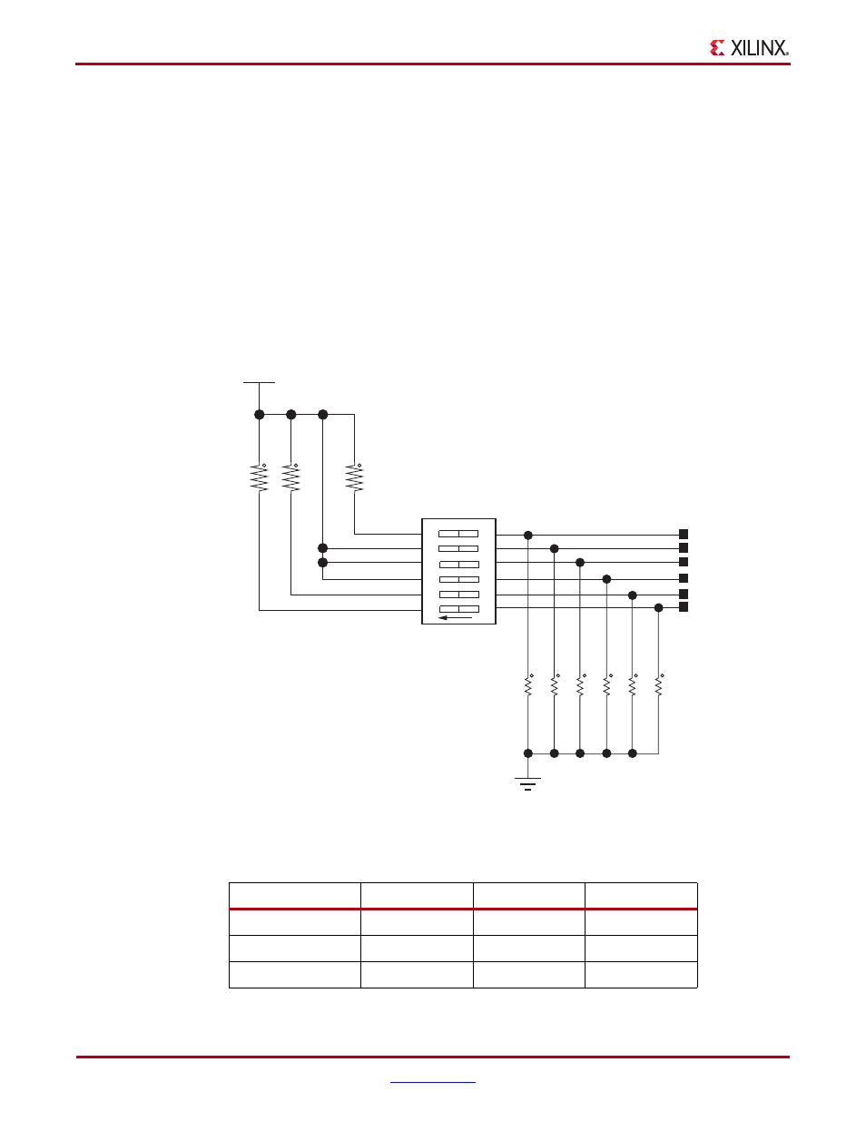
DIP switch S2 is a multi-purpose selector switch (
FPGA Mode:
S2 switches 3, 4, and 5 control the FPGA mode (
).
Oscillator Enable:
S2 switch 1, CCLK_EXTERNAL, controls the enable pin of the 47 MHz
oscillator SiT8102 (X4). When switch 1 is closed (CCLK_EXTERNAL High), X4 drives a
47 MHz clock onto the FPGA_CCLK signal.
Boot EEPROM Select:
S2 switch 2 is used to select the between the Xilinx Platform Flash or
the Numonyx Linear BPI Flash for the FPGA boot memory device.
Upper or Lower Address Select:
S2 switch 6 is used to select the upper or lower half of
flash memory U4 as the source of the FPGA bitstream image. When FLASH_A23 is High,
the upper half of the address is selected. When FLASH_A23 is Low, the lower half of the
address is selected.
shows the FPGA configuration modes controlled by S2 switches 3, 4, and 5.
X-Ref Target - Figure 1-27
Figure 1-27:
Multi-Purpose Select DIP Switch S2
Table 1-26:
ML605 Configuration Modes
Configuration Mode
M[2:0]
Bus Width
CCLK
Master BPI-Up
010
8, 16
Output
JTAG
101
1
Input (TCK)
Slave SelectMAP
110
8, 16, 32
Input
UG534_27_110409
SDMX-6-X
4
5
6
12
3
4
56
9
8
7
1
2
3
12
11
10
S2
ON
VCC2V5
1
2
5%
1/16W
510
R57
1/16W
5%
1
2
5%
1/16W
510
R52
2
1
R51
510
1/16W
5%
CCLK EXTERNAL
P30_CS_SEL
FPGA_M0
FPGA_M1
FPGA_M2
FLASH_A23
1
2
1
2
1
2
1
2
1
2
1
2
1/16w
5%
1/16w
5%
1/16w
5%
1/16w
5%
1/16w
5%
1/16w
5%
R4
3
R50
R5
3
R54
R55
R56
4.7K
4.7K
4.7K
4.7K
4.7K
4.7K