Detailed description, Figure 1-2, Updated – Xilinx ML605 User Manual
Page 13
ML605 Hardware User Guide
13
UG534 (v1.8) October 2, 2012
Detailed Description
Detailed Description
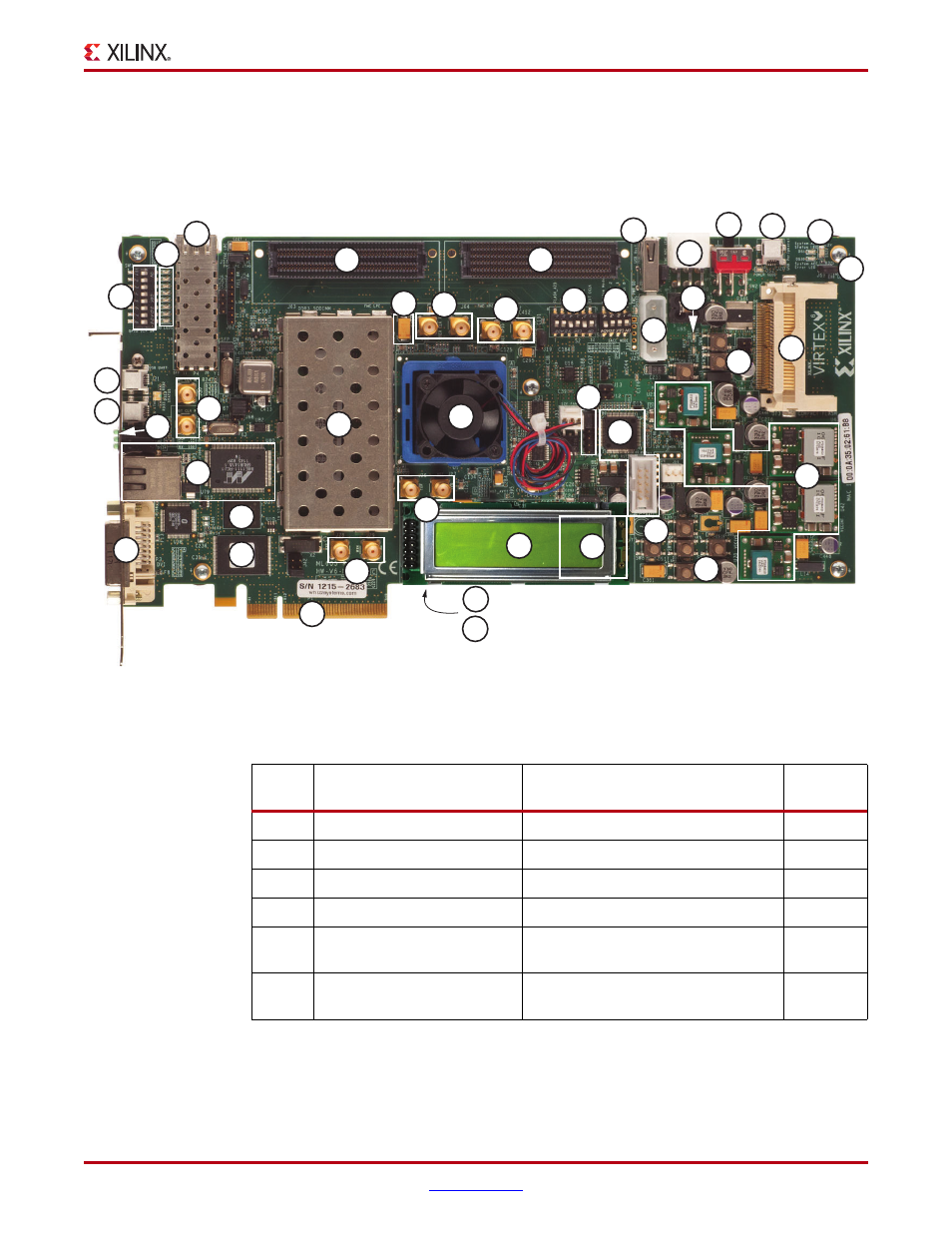
shows a board photo with numbered features corresponding to
the section headings in this document.
The numbered features in
correlate to the features and notes listed in
X-Ref Target - Figure 1-2
Figure 1-2:
ML605 Board Photo
1
2
13
5
10
15
13
16b
16c
23
19
18a
18b
18c
18
d
17c
17b
17f
21a
21a
21b
21c
21d
22
7a
(on backside)
17a
17
d
20
12
6
16a
7d
11
14
3
4
9
UG534_02_091312
7c
17e
7b
8
8
Table 1-1:
ML605 Features
Number
Feature Notes
Schematic
Page
1
Virtex-6 FPGA
XC6VLX240T-1FFG1156
2 - 12
2
DDR3 SODIMM
Micron 512 MB MT4JSF6464HY-1G1
15
3
128 Mb Platform Flash XL
Xilinx XCF128X-FTG64C
25
4
Linear BPI Flash
Numonyx JS28F256P30T95
26
5
System ACE CF controller, CF
connector
Xilinx XCCACE-TQ144I
(bottom of board)
13
6
JTAG cable connector (USB
Mini-B)
USB JTAG download circuit
46