128 mb platform flash xl, 32 mb linear bpi flash, Figure 1-3 – Xilinx ML605 User Manual
Page 22: 128 mb platform flash xl 4. 32 mb linear bpi flash
22
ML605 Hardware User Guide
UG534 (v1.8) October 2, 2012
Chapter 1: ML605 Evaluation Board
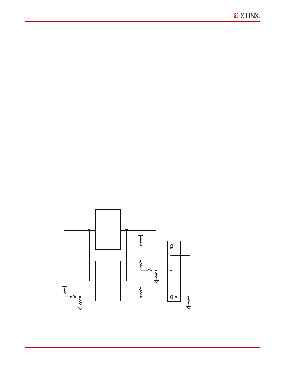
3. 128 Mb Platform Flash XL
A 128 Mb Xilinx XCF128X-FTG64C Platform Flash XL device is used with an onboard
47 MHz oscillator (X4) to configure the FPGA in less than 100 ms from power valid as
required by the PCI Express Card Electromechanical Specification. This allows the PCIe
interface to be recognized and enumerated when plugged into a host PC.
To achieve the fastest configuration speed, the FPGA mode pins are set to Slave SelectMAP
and the onboard 47 MHz clock source external to the FPGA is used for configuration.
Configuration DIP switch S2, switch 1, controls the 47 MHz oscillator enable as outlined in
.
See S2 switch setting details in
. Also, see the
Considerations for the Configuration Flash, page 25
for FPGA design recommendations.
4. 32 MB Linear BPI Flash
A Numonyx JS28F256P30 Linear BPI Flash memory (P30) on the ML605 provides 32 MB of
non-volatile storage that can be used for configuration as well as software storage. The
Linear BPI Flash shares the dual use configuration pins in parallel with the XCF128
Platform Flash XL.
The P30_CS net is used to select the P30 or the XCF128. Power-on configuration is selected
by the P30_CS net which is tied to a dip switch S2 (selects pullup/pulldown) and is also
wired to an FPGA non-config pin. The dip switch allows power selection for the
configuration device P30 or XCF128XL. The dip switch selection can be overridden by the
FPGA after configuration by controlling the logic level of the P30_CS signal.
See S2 switch setting details in
. For an overview on configuring the
FPGA, see
Configuration Options, page 76
.
shows a block diagram for the Platform Flash and BPI Flash.
X-Ref Target - Figure 1-3
Figure 1-3:
Platform Flash and BPI Flash Block Diagram
UG534_03_011110
FPGA U1
Bank 34
FLASH_A[22:0]
FPGA U1
Bank 24
FLASH_A[23]
FLASH_D[15:0]
U4
U27
BPI
FLASH
PLATFORM
FLASH
A
D
A
A23
D
CE
E
FPGA U1
Bank 24
U10
VCC2V5
VCC2V5
VCC2V5
PLATFLASH_FCS_B
FLASH_CE_B
FPGA_FCS_B
FPGA U1
Bank 24
S2 SWITCH 2
ON = U4 BOOT
OFF = U27 BOOT
1
6
4
3
11
S2-2
2
VCC2V5
7
S2-6
510
4.7K
510
4.7K
6
S2 SWITCH 6
ON = U4 BPI Upper Half
OFF = U4 BPI Lower Half
P30_CS_SEL
(FPGA U1 pin AJ12)
S1 Switch 4
OFF = Disable System ACE,
enable U4/U27 flash boot
ON = Enable System ACE boot when
CF card is present