Xilinx ChipScope PLB46 IBA v1.00a User Manual
Page 9
DS619 April 7, 2009
9
Product Specification
G46
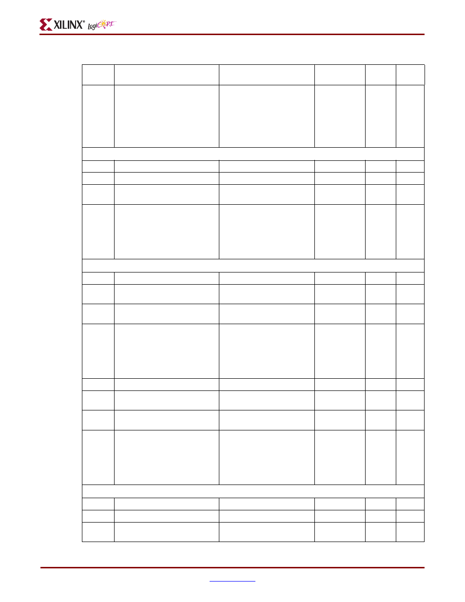
1=Enable storing MU 6 signals in
the data sample storage buffer.
0=Disable
C_USE_MU_6A_SLV_CTL or
C_USE_MU_6B_SLV_SZ_WADD
R must be 1 in order to store.
C_MU_6_EN_STORE_SLV_
CTL_BUS
0,1
1
Integer
Slave Busy Status
G47
USE SI_MBusy signal
C_USE_MU_7_SLV_BSY
1,0
0
Integer
G48
0=basic, 1=basic w/ edges
C_MU_7_TYPE_SLV_BSY
0,1
0
Integer
G49
Match unit counter width. 0 means
do not use
C_MU_7_CNT_W_SLV_BSY
0,1-32
0
Integer
G50
1=Enable storing MU 7 signals in
the data sample storage buffer.
0=Disable
C_USE_MU_7_SLV_BSY must be
1 in order to store.
C_MU_7_EN_STORE_SLV_
BSY
0,1
1
Integer
Slave Read/Writer Error Status
G51
Use SI_MRdErr
C_USE_MU_8_SLV_RD_ERR
1,0
0
Integer
G52
0=basic, 1=basic w/ edges
C_MU_8_TYPE_SLV_RD_
ERR
0,1
0
Integer
G53
Match unit counter width. 0 means
do not use
C_MU_8_CNT_W_SLV_RD_
ERR
0,1-32
0
Integer
G54
1=Enable storing MU 8 signals in
the data sample storage buffer.
0=Disable
C_USE_MU_8_SLV_RD_ERR
must be 1 in order to store.
C_MU_8_EN_STORE_SLV_
RD_ERR
0,1
1
Integer
G55
Use SI_MWrErr
C_USE_MU_9_SLV_WR_ERR 1,0
0
Integer
G56
0=basic, 1=basic w/ edges
C_MU_9_TYPE_SLV_WR_
ERR
0,1
0
Integer
G57
Match unit counter width. 0 means
do not use
C_MU_9_CNT_W_SLV_WR_
ERR
0,1-32
0
Integer
G58
1=Enable storing MU 9 signals in
the data sample storage buffer.
0=Disable
C_USE_MU_9_SLV_WR_ERR
must be 1 in order to store.
C_MU_9_EN_STORE_SLV_
WR_ERR
0,1
1
Integer
PLB Arbitration
G59
Use Master arbitration signals
C_USE_MU_10_ARB_CTL
1,0
0
Integer
G60
0=basic, 1=basic w/ edges
C_MU_10_TYPE_ARB_CTL
0,1
0
Integer
G61
Match unit counter width. 0 means
do not use
C_MU_10_CNT_W_ARB_CTL 0,1-32
0
Integer
Table 2: IBA_PLBv46 Design Parameters (Cont’d)
Generic
Feature/Description
Parameter Name
Allowable
Values
Default
Value
VHDL
Type