Xilinx ChipScope PLB46 IBA v1.00a User Manual
Page 7
DS619 April 7, 2009
7
Product Specification
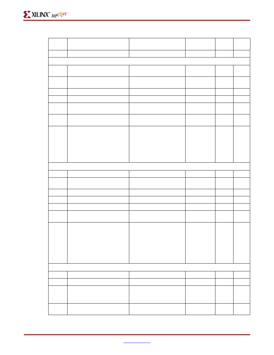
G13
Enable Trigger Out
C_ENABLE_TRIGGER_OUT
1,0
0
Integer
Trigger In, PLB Reset, and PLB Error Status
G14
Use system reset and error status
signals
C_USE_MU_1A_RST_ERR_
STAT
1,0
1
Integer
G15
Use master error status signals
C_USE_MU_1B_MSTR_RST_
ERR_STAT
1,0
0
Integer
G16
Use iba_trig_in
C_USE_MU_1C_TRIG_IN
1,0
0
Integer
G17
Trigger in width, 0=disable
C_MU_1_TRIG_IN_WIDTH
0-189
0
Integer
G18
0=basic, 1=basic w/ edges
C_MU_1_TYPE_TRIG_RST_
ERR_STAT
0,1
1
Integer
G19
Match unit counter width. 0 means
do not use.
C_MU_1_CNT_W_TRIG_
RST_ERR_STAT
0,1-32
0
Integer
G20
1=Enable storing MU 1 signals in
the data sample storage buffer.
0=Disable
C_USE_MU_1A or
C_USE_MU_1B must be 1 in order
to store.
C_MU_1_EN_STORE_TRIG_
RST_ERR_STAT
0,1
1
Integer
PLB Grouped Control Bus
G21
Use the grouped control bus signals C_USE_MU_2A_STD_CTL
1,0
1
Integer
G22
Use the grouped size and byte enable
signals
C_USE_MU_2B_SIZE_BE
1,0
1
Integer
G23
Use PLB_TAttribute signals
C_USE_MU_2C_TATTR
1,0
1
Integer
G24
Number of match units to use
C_MU_2_NUM_GRP_CTL
1,2
1
Integer
G25
0=basic, 1=basic w/ edges
C_MU_2_TYPE_GRP_CTL
0,1
0
Integer
G26
Match unit counter width. 0 means
do not use
C_MU_2_CNT_W_GRP_CTL
0,1-32
0
Integer
G27
1=Enable storing MU 2 signals in
the data sample storage buffer.
0=Disable
C_USE_MU_2A_STD_CTL or
C_USE_MU_2B_SIZE_BE or
C_USE_MU_2C_TATTR must be 1
in order to store.
C_MU_2_EN_STORE_GRP_
CTL
0,1
1
Integer
PLB Address
G28
Use PLB_ABus
C_USE_MU_3A_ABUS
1,0
1
Integer
G29
Use PLB_UABus
C_USE_MU_3B_UABUS
1,0
1
Integer
G30
0=basic, 1=basic w/ edges,
2=extended, 3= extended w/edges,
4=range, 5=range w/edges
C_MU_3_TYPE_ADDR
0,1,2,3,4,5
0
Integer
G31
Match unit counter width. 0 means
do not use
C_MU_3_CNT_W_ADDR
0,1-32
0
Integer
Table 2: IBA_PLBv46 Design Parameters (Cont’d)
Generic
Feature/Description
Parameter Name
Allowable
Values
Default
Value
VHDL
Type