Xilinx ChipScope PLB46 IBA v1.00a User Manual
Page 8
8
DS619 April 7, 2009
Product Specification
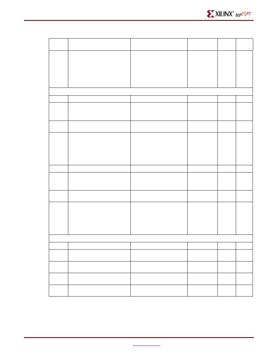
G32
1=Enable storing MU 3 signals in
the data sample storage buffer.
0=Disable
C_USE_MU_3A_ABUS or must
C_USE_MU_3B_UABUS be 1 in
order to store.
C_MU_3_EN_STORE_ADDR
0,1
1
Integer
PLB Data
G33
Use PLB_wrDBus
C_USE_MU_4_WR_DBUS
1,0
0
Integer
G34
0=basic, 1=basic w/ edges,
2=extended, 3= extended w/edges,
4=range, 5=range w/edges
C_MU_4_TYPE_WR_DBUS
0,1,2,3,4,5
0
Integer
G35
Match unit counter width. 0 means
do not use.
C_MU_4_CNT_W_WR_DBUS 0,1-32
0
Integer
G36
1=Enable storing MU 4 signals in
the data sample storage buffer.
0=Disable
C_USE_MU_4_WR_DBUS must
be 1 in order to store.
C_MU_4_EN_STORE_WR_
DBUS
0,1
1
Integer
G37
Use PLB_srdDBus
C_USE_MU_5_RD_DBUS
1,0
1
Integer
G38
0=basic, 1=basic w/ edges,
2=extended, 3= extended w/edges,
4=range, 5=range w/edges
C_MU_5_TYPE_RD_BUS
0,1,2,3,4,5
0
Integer
G39
Match unit counter width. 0 means
do not use
C_MU_5_CNT_W_RD_DBUS
0,1-32
0
Integer
G40
1=Enable storing MU 5 signals in
the data sample storage buffer.
0=Disable
C_USE_MU_5_RD_DBUS must be
1 in order to store.
C_MU_5_EN_STORE_RD_
DBUS
0,1
1
Integer
Slave Control Bus
G41
Use Slave Congrol signals
C_USE_MU_6A_SLV_CTL
1,0
0
Integer
G42
USE SI_rdWdAddr and SI_SSize
C_USE_MU_6B_SLV_SZ_
WADDR
1,0
0
Integer
G43
Number of match units to use
C_MU_6_NUM_SLV_CTL_
BUS
1,2
0
Integer
G44
0=basic, 1=basic w/ edges
C_MU_6_TYPE_SLV_CTL_
BUS
0,1
0
Integer
G45
Match unit counter width. 0 means
do not use
C_MU_6_CNT_W_SLV_CTL_
BUS
0,1-32
0
Integer
Table 2: IBA_PLBv46 Design Parameters (Cont’d)
Generic
Feature/Description
Parameter Name
Allowable
Values
Default
Value
VHDL
Type