Specifi cations (continued), Other s, List of supported signals (component signals) – Toshiba TDP-TW420 User Manual
Page 50: List of supported signals (video, s-video signals), Pin assignment of dvi-i terminal
98
99
Other
s
List of supported signals (Component signals)
Signal format
fh(kHz)
fv(Hz)
480i(525i)@60Hz
*
15.73
59.94
480p(525p)@60Hz
31.47
59.94
576i(625i)@50Hz
*
15.63
50.00
576p(625p)@50Hz
31.25
50.00
720p(750p)@60Hz
45.00
60.00
720p(750p)@50Hz
37.50
50.00
1080i(1125i)@60Hz
33.75
60.00
1080i(1125i)@50Hz
28.13
50.00
1080p(1125p)@60Hz
67.50
60.00
1080p(1125p)@50Hz
56.25
50.00
* DVI digital input is not supported.
List of supported signals (Video, S-Video signals)
Video mode
fh(kHz)
fv(Hz)
fsc(MHz)
NTSC
15.73
60
3.58
PAL
15.63
50
4.43
SECAM
15.63
50
4.25 or 4.41
PAL-M
15.73
60
3.58
PAL-N
15.63
50
3.58
PAL-60
15.73
60
4.43
NTSC4.43
15.73
60
4.43
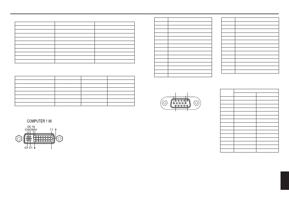
Pin assignment of DVI-I terminal
■
■
■
Analog input signal
Analog RGB input
RGB signals:
0.7 V (p-p) 75
:
Horizontal sync signal: TTL level (Pos/neg polarity)
Vertical sync signal: TTL level (Pos/neg polarity)
Y/P
B
/P
R
input
Y signal:
1.0 V (p-p) 75
:
P
B
/P
R
signals:
0.7 V (p-p) 75
:
•
•
DVI digital & analog connector
Specifi cations (Continued)
Pin assignment of COMPUTER 2 IN & MONITOR terminals
Pin No.
Pin description
During RGB input During Y/P
B
/P
R
input
1
Video signal (R)
Color difference signal (P
R
)
2
Video signal (G)
Luminance signal (Y)
3
Video signal (B)
Color difference signal (P
B
)
4
GND
*
5
GND
*
6
GND(R)
GND(P
R
)
7
GND(G)
GND(Y)
8
GND(B)
GND(P
B
)
9
N.C
*
10
GND
*
11
GND
*
12
N.C
*
13
Horizontal sync signal *
14
Vertical sync signal *
15
N.C
*
* Do not connect anything.
■
Input Signal
RGB input
RGB signals:
0.7 V (p-p) 75
:
Horizontal sync signal: TTL level (Pos/neg polarity)
Vertical sync signal: TTL level (Pos/neg polarity)
Y/P
B
/P
R
input
Y signal:
1.0 V (p-p) 75
:
P
B
/P
R
signals:
0.7 V (p-p) 75
:
•
•
Mini D sub 15 Pin connector
5
1
10
15
11
6
Pin No.
Pin description
Pin No.
Pin description
1
T.M.D.S. data 2 –
16
Hot plug detection
2
T.M.D.S. data 2 +
17
T.M.D.S. data 0 –
3
T.M.D.S. data 2/4 shielded
18
T.M.D.S. data 0 +
4
T.M.D.S. data 4 – (N.C)
19
T.M.D.S. data 0/5 shielded
5
T.M.D.S. data 4 + (N.C)
20
T.M.D.S. data 5 – (N.C)
6
DDC clock
21
T.M.D.S. data 5 + (N.C)
7
DDC data
22
T.M.D.S. clock shielded
8
Analog vertical sync signal
23
T.M.D.S. clock +
9
T.M.D.S. data 1 –
24
T.M.D.S. clock –
10
T.M.D.S. data 1 +
C1
Analog video signal (R/P
R
)
11
T.M.D.S. data 1/3 shielded
C2
Analog video signal (G/Y)
12
T.M.D.S. data 3 – (N.C)
C3
Analog video signal (B/P
B
)
13
T.M.D.S. data 3 + (N.C)
C4
Analog horizontal sync signal
14
+5 V power source
C5
Analog GND (R/P
R
, G/Y, B/P
B
)
15
GND(+5 V, H Sync & V Sync)