6 sdram timing 2 register (sdtim2), Section 4.6 – Texas Instruments TMS320C6455 User Manual
Page 46
DDR2 Memory Controller Registers
4.6
SDRAM Timing 2 Register (SDTIM2)
Like the SDRAM timing 1 register (SDTIM1), the SDRAM timing 2 register (SDTIM2) also configures the
DDR2 memory controller to meet the AC timing specification of the DDR2 memory. For information on the
appropriate values to program each field, see the DDR2 memory section of the device-specific data
manual. The bit fields in the SDTIM2 register are only writeable when the TIMUNLOCK bit of the SDRAM
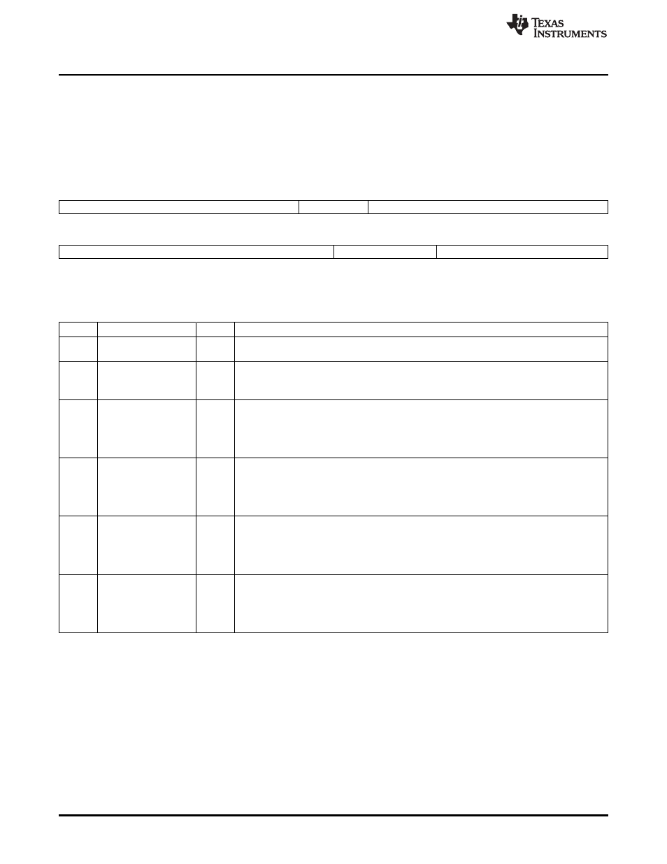
Configuration register (SDCFG) is unlocked. SDTIM2 is shown in
and described in
Figure 24. SDRAM Timing 2 Register (SDTIM2)
31
25
24
23
22
16
Reserved
T_ODT
T_XSNR
R-0x0
R/W-0x3
R/W-0x7F
15
8
7
5
4
0
T_XSRD
T_RTP
T_CKE
R/W-0xFF
R/W-0x7
R/W-0x1F
LEGEND: R/W = Read/Write; R = Read only; -n = value after reset; -x = value is indeterminate after reset
Table 23. SDRAM Timing 2 Register (SDTIM2) Field Descriptions
Bit
Field
Value
Description
31-25
Reserved
Reserved. The reserved bit location is always read as 0. A value written to this field has no
effect.
24-23
T_ODT
Minimum number of DDR clock cycles from ODT enable to write data driven for DDR2
SDRAM. T_ODT must be equal to t
AOND
.
T_ODT = t
AOND
22-16
T_XSNR
0-7Fh
These bits specify the minimum number of DDR2CLKOUT cycles from a self_refresh exit to
any other command except a read command, minus 1. The value for these bits can be derived
from the t
XSNR
AC timing parameter in the DDR2 section of the device-specific data manual.
Calculate using this formula:
T_XSNR = t
XSNR
- 1
15-8
T_XSRD
0-FFh
These bits specify the minimum number of DDR2CLKOUT cycles from a self_refresh exit to a
read command, minus 1. The value for these bits can be derived from the t
XSRD
AC timing
parameter in the DDR2 section of the device-specific data manual. Calculate using this
formula:
T_XSRD = t
XSRD
- 1
7-5
T_RTP
0-7h
These bits specify the minimum number of DDR2CLKOUT cycles from a last read command
to a precharge command, minus 1. The value for these bits can be derived from the t
rtp
AC
timing parameter in the DDR2 section of the device-specific data manual. Calculate using this
formula:
T_RTP = (t
rtp
/DDR2CLKOUT) - 1
4-0
T_CKE
0-1Fh
These bits specify the minimum number of DDR2CLKOUT cycles between transitions on the
DSDCKE pin, minus 1. The value for these bits can be derived from the t
cke
AC timing
parameter in the DDR2 section of the device-specific data manual. Calculate using this
formula:
T_CKE = t
cke
- 1
46
C6455/C6454 DDR2 Memory Controller
SPRU970G
–
December 2005
–
Revised June 2011
Copyright
©
2005
–
2011, Texas Instruments Incorporated