Texas Instruments TMS320C6455 User Manual
Page 12
DED[31:0]
DDR2
Memory
Controller
DDR2CLKOUT
DDR2CLKOUT
DCE0
DSDCKE
DSDRAS
DSDWE
DSDDQM[3:0]
DSDCAS
DBA[2:0]
DSDDQS[3:0]
DEA[13:0]
V
REFSSTL
DSDDQGATE[3:0]
DSDDQS[3:0]
DEODT[1:0]
DDRSLRATE
Peripheral Architecture
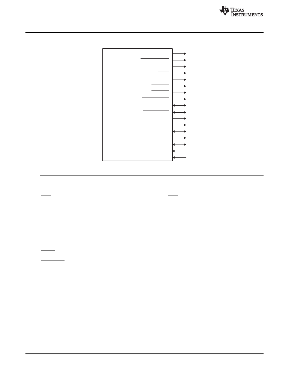
Figure 2. DDR2 Memory Controller Signals
Table 1. DDR2 Memory Controller Signal Descriptions
Pin
Description
DED[31:0]
Bidirectional data bus. Input for data reads and output for data writes.
DEA[13:0]
External address output.
DCE0
Active-low chip enable for memory space CE0. DCE0 is used to enable the DDR2 SDRAM memory
device during external memory accesses. The DCE0 pin stays low throughout the operation of the
DDR2 memory controller; it never goes high. Note that this behavior does not affect the ability of the
DDR2 memory controller to access DDR2 SDRAM memory devices.
DSDDQM[3:0]
Active-low output data mask.
DDR2CLKOUT
Differential clock outputs.
DDR2CLKOUT
DSDCKE
Clock enable (used for self-refresh mode).
DSDCAS
Active-low column address strobe.
DSDRAS
Active-low row address strobe.
DSDWE
Active-low write enable.
DSDDQS[3:0]/
Differential data strobe bidirectional signals.
DSDDQS[3:0]
DEODT[1:0]
On-die termination signals to external DDR2 SDRAM. These pins are reserved for future use and
should not be connected to the DDR2 SDRAM.
DBA[2:0]
Bank-address control outputs.
DSDDQGATE[3:0]
Data strobe gate pins. These pins are used as a timing reference during memory reads. The
DSDDQGATE0 and DSDDQGATE2 pins should be routed out and connected to the DSDDQGATE1
and DSDDQGATE3 pins, respectively. For more routing requirements on these pins, see the
device-specific data manual.
V
REFSSTL
DDR2 Memory Controller reference voltage. This voltage must be supplied externally. For more details,
see the device-specific data manual.
DDRSLRATE
Pulling the DDRSLRATE input pin low selects the normal slew rate. If pulled high, the slew rate is
reduced by 33%. For normal full-speed operation, the DDRSLRATE should be pulled low.This pin
needs to be pulled low or high at all times (it is not latched).
12
C6455/C6454 DDR2 Memory Controller
SPRU970G
–
December 2005
–
Revised June 2011
Copyright
©
2005
–
2011, Texas Instruments Incorporated