Debug lcd module, Option links – Renesas Single-Chip Microcomputer H8/36079 User Manual
Page 12
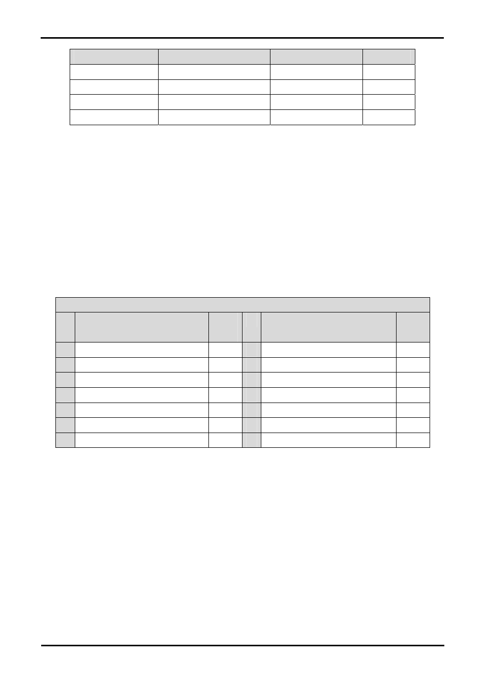
Description
Function
Circuit Net Name
Device Pin
SCI3
Programming serial port
TxD
46
SCI3
Programming serial port
RxD
45
SCI3_2
Spare Serial Port
TxD2
50
SCI3_2
Spare Serial Port
RxD2
49
Table 6-3: Serial Port settings
The SCI3_2 port is also available on J4 and JA2. The SCI3 port is available on J3.
6.5. Debug LCD Module
A debug LCD module is supplied to be connected to the connector LCD. This should be fitted so that the debug LCD module lies over J1.
Care should be taken to ensure the pins are inserted correctly into LCD. The debug LCD module uses a 4 bit interface to reduce the pin
allocation. No contrast control is provided; this is set by a resistor on the supplied display module. The module supplied with the RSK only
supports 5V operation.
Table 6-4 shows the pin allocation and signal names used on this connector.
LCD
Pin
Circuit Net Name
Device
Pin
Pin
Circuit Net Name
Device
Pin
1 Ground
-
2 5V
Only
-
3 No
Connection
-
4 DLCDRS
(P24)
31
5
R/W (Wired to Write only)
-
6
DLCDE+ 100k pull down to ground (P12)
25
7 No
Connection
-
8 No
connection
-
9 No
Connection
-
10 No
connection
-
11 DLCDD4
(P50)
13
12 DLCDD5
(P51)
14
13 DLCDD6
(P52)
19
14 DLCDD7
(P53)
20
Table 6-4 Debug LCD Module Connections
6.6. Option Links
Table 6-5 below describes the function of the option links associated with E8A configuration. The default configuration is indicated by
BOLD text.
8