NEC uPD78056Y User Manual
Page 569
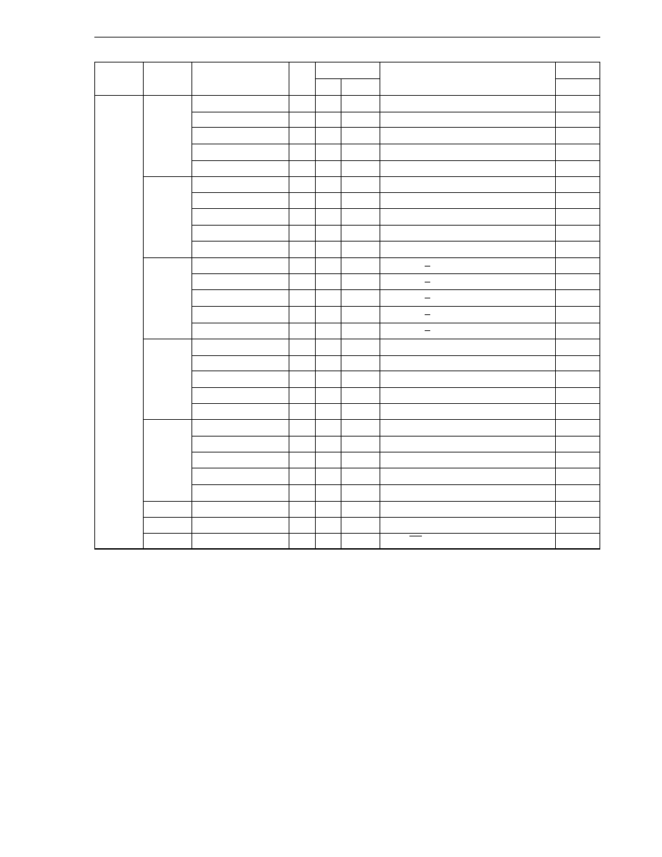
569
CHAPTER 27 INSTRUCTION SET
Clock
Flag
Note 1
Note 2
Z AC CY
CY, saddr.bit
3
6
7
CY
←
CY
∧
(saddr.bit)
×
CY, sfr.bit
3
–
7
CY
←
CY
∧
sfr.bit
×
AND1
CY, A.bit
2
4
–
CY
←
CY
∧
A.bit
×
CY, PSW.bit
3
–
7
CY
←
CY
∧
PSW.bit
×
CY, [HL].bit
2
6
7 + n
CY
←
CY
∧
(HL).bit
×
CY, saddr.bit
3
6
7
CY
←
CY
∨
(saddr.bit)
×
CY, sfr.bit
3
–
7
CY
←
CY
∨
sfr.bit
×
OR1
CY, A.bit
2
4
–
CY
←
CY
∨
A.bit
×
CY, PSW.bit
3
–
7
CY
←
CY
∨
PSW.bit
×
CY, [HL].bit
2
6
7 + n
CY
←
CY
∨
(HL).bit
×
CY, saddr.bit
3
6
7
CY
←
CY
∨
(saddr.bit)
×
CY, sfr.bit
3
–
7
CY
←
CY
∨
sfr.bit
×
XOR1
CY, A.bit
2
4
–
CY
←
CY
∨
A.bit
×
CY, PSW. bit
3
–
7
CY
←
CY
∨
PSW.bit
×
CY, [HL].bit
2
6
7 + n
CY
←
CY
∨
(HL).bit
×
saddr.bit
2
4
6
(saddr.bit)
←
1
sfr.bit
3
–
8
sfr.bit
←
1
SET1
A.bit
2
4
–
A.bit
←
1
PSW.bit
2
–
6
PSW.bit
←
1
Ч Ч Ч
[HL].bit
2
6
8 + n + m
(HL).bit
←
1
saddr.bit
2
4
6
(saddr.bit)
←
0
sfr.bit
3
–
8
sfr.bit
←
0
CLR1
A.bit
2
4
–
A.bit
←
0
PSW.bit
2
–
6
PSW.bit
←
0
Ч Ч Ч
[HL].bit
2
6
8 + n + m
(HL).bit
←
0
SET1
CY
1
2
–
CY
←
1
1
CLR1
CY
1
2
–
CY
←
0
0
NOT1
CY
1
2
–
CY
←
CY
×
Notes 1. When the internal high-speed RAM area is accessed or instruction with no data access.
2. When an area except the internal high-speed RAM area is accessed.
Remarks 1. One instruction clock cycle is one cycle of the CPU clock (f
CPU
) selected by the processor clock
control register (PCC).
2. This clock cycle applies to internal ROM program.
3. n is the number of waits when external memory expansion area is read from.
4. m is the number of waits when external memory expansion area is written to.
Mnemonic
Operands
Byte
Operation
Instruction
Group
Bit
manipulate