3 power sequencing – Nvidia TEGRA DG-04927-001_V01 User Manual
Page 18
Tegra 200 Series Developer Board User Guide
DG-04927-001_v01
Advance Information – Subject to Change
18
NVIDIA CONFIDENTIAL
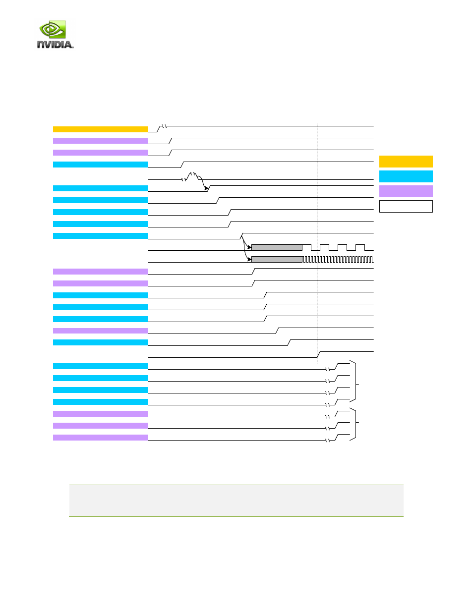
4.1.3 Power Sequencing
The Power solution, including the PMU and any external supplies/logic, must be able to meet the Tegra 250 power sequence
requirements. These requirements are detailed in the Tegra 200 Series datasheet (Electrical, Mechanical and Thermal
Specifications). Figure 7 shows the sequence used for the Smartbook Development System.
Figure 7. Power-up Sequence Example
VDDIO_SYS/AVDD_OSC (1.8V, PMU LDO4)
VDD_RTC (1.2V, PMU LDO2)
AVDD_USB / USB_PLL (3.3V, PMU LDO3)
VDD_CPU (1.0V, PMU SM1)
VDD_CORE (1.2V, PMU SM0)
CLK_32K_IN (PMU)
System Clock (External Source or XTAL)
VDD_DDR_RX (2.85V, PMU LDO9)
32KHz Ramp Time
VBAT (10.2-12.6V, 15V)
VDD_5V0 (5V, DC/DC TPS51220A)
VDD_3V3_SBY (3.3V, DC/DC TPS51220A)
VDD_3V3 (3.3V, DC/DC TPS51220A)
VDD_1V05 (1.05V, DC/DC TPS62290)
V2REF_DDR2 (0.9V, DC/DC TPS51116)
VDD_1V8 (1.8V, DC/DC TPS51116)
AVDD_DSI_CSI (1.2V, LDO TPS72012)
VDDIO_ONKEY (2.2V, PMU LDO)
ONKEY (VDD_2V2)
VDD_SM2 (3.7V, PMU SM2)
VCORE_MMC (2.85V, PMU LDO5)
AVDD_PLL (1.1V, PMU LDO1)
Oscillator Ramp Time
VDD_3V3: VDDIO_NAND_3V3, VDDIO_SDIO,VDDIO_VI
SYS_RESET_N (PMU)
VDD_1V8: VDDIO_NAND_1V8, VDDIO_LCD, VDDIO_BB, VDDIO_AUDIO, VDDIO_UART, VDDIO_DDR
Misc. 1.5V, 3.3V, 5.0V, Backlight
GPIO
Enabled
VDD_1V05: AVDD_PLLE, AVDD_PEX, AVDD_PEX_PLL, VDD_PEX
BATTERY or AC/DC
EXTERNAL SUPPLY
PMU SUPPLY
AVDD_VDAC (2.85V, PMU LDO6)
AVDD_HDMI (3.3V, PMU LDO7)
AVDD_HDM_PLL (1.8V, PMU LDO8)
VDDIO_PEX_CLK (3.3V, PMU LDO0)
Off by
Default
Signals
Note:
1: VDD_RTC, VDD_CORE, Critical PLLs, AVDD_OSC, VDDIO_SYS, VDDIO_DDR, VDDIO_NAND, 32.768KHz
and System clocks required before SYS_RESET_N goes high
2: Recommended Power-down sequence is reverse of Power-up.