Figure d-11. vxibus connectors location and pinout, Table d-10. vxibus p2 connector signals, Vxibus p1 and p2 – National Instruments 800 Series User Manual
Page 68
Appendix D
Front Panel and Connectors
© National Instruments Corporation
D-17
VXIpc 800 Series User Manual
VXIbus P1 and P2
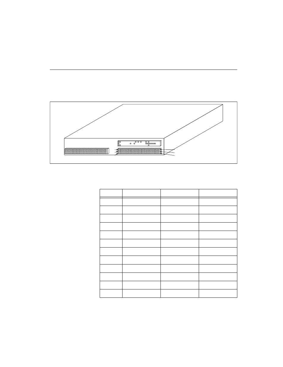
Figure D-11 shows the location and pinouts for the VXIbus connector
on the VXIpc 800 Series. Table D-10 gives the name and description for
the VXIbus P2 connector signals. Table D-11 gives the name and
description for the VXIbus P1 connector signals.
Figure D-11. VXIbus Connectors Location and Pinout
Table D-10. VXIbus P2 Connector Signals
Pin
Row C
Row B
Row A
1
CLK10+
+5 V
ECLTRG0
2
CLK10-
GND
–2 V
3
GND
Not Connected
ECLTRG1
4
–5.2 V
A24
GND
5
Not Connected
A25
MODID12
6
Not Connected
A26
MODID11
7
GND
A27
–5.2 V
8
Not Connected
A28
MODID10
9
Not Connected
A29
MODID09
10
GND
A30
GND
11
Not Connected
A31
MODID08
12
Not Connected
GND
MODID07
P1 Connector
P2 Connector
C1
B1
A1
C32
B32
A32