Partial circuit switch down, Nxp semiconductors – NXP Semiconductors UM10301 PCF2123 User Manual
Page 38

NXP Semiconductors
UM10301
User Manual PCF85x3, PCA8565 and PCF2123, PCA2125
UM10301_1
© NXP B.V. 2008. All rights reserved.
User manual
Rev. 01 — 23 December 2008
38 of 52
001aai849
SMD
CRYSTAL
SDA
CLK
V
DD
SCL
V
SS
OSCO
OSCI
INT
layer 1
ground via
GND area
PCF8563TS
bypass
capacitor
oscillator
capacitor
guard ring
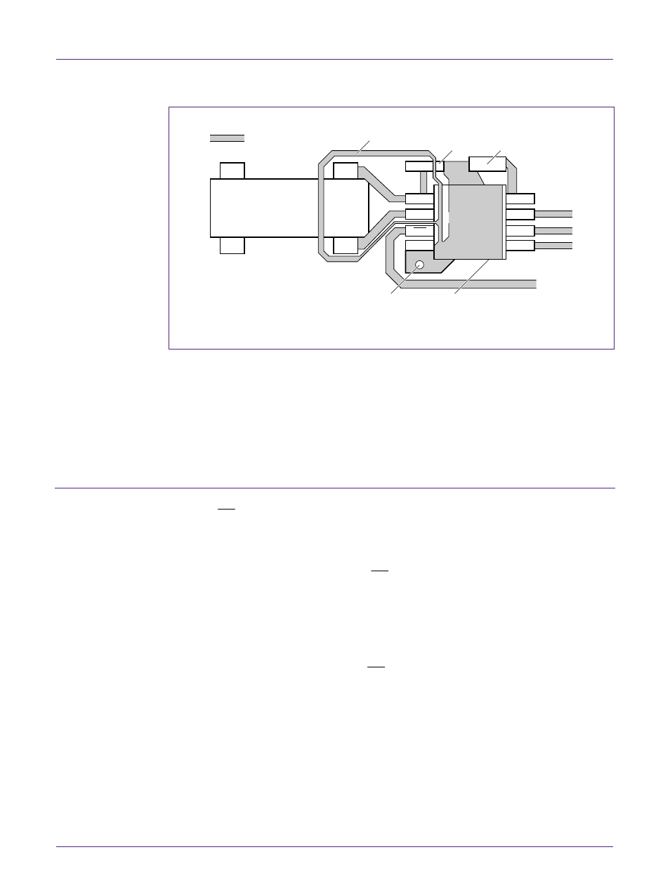
Fig 15. PCB layout proposal for PCF8563 using SMD components and guard ring
Remark: Take precautions when cleaning PCBs containing tuning fork crystals using
ultrasound. The resonance vibration may damage the crystal. Consult the supplier of the
crystal in case of doubt.
15. Partial circuit switch down
The I
2
C-bus RTC circuits PCF8563, PCA8565 and PCF8593 have on the pads SDA,
SCL and
INT
a diode clamping circuit without an upper clamping diode to V
DD
, refer to
Therefore it is possible to partially switch off V
DD
such that the RTC is powered down or
working at a lower supply voltage than the rest of the circuit without the risk that via such
(upper) clamping diodes SDA, SCL and INT would be pulled down as well.
The other way around with only the RTC powered in order to keep time and the rest of
the circuit switched off will be a more common situation. If during normal operation the
complete application is powered by a certain V
DD
of for example 3.3 V or 5 V, then during
standby just the RTC can be operating and powered from a backup source as discussed
in Chapter 13. See Fig 16 and Fig 18 plus Fig 19.
PCF8583 has no protection diode from
INT
to V
DD
but has protection diodes from the I
2
C-
bus pins to V
DD
! Battery backup will work, but with the RTC powered down the I
2
C-bus
may get stuck.
The SPI-bus RTC circuits PCF2123 and PCA2125 have on pins SDI and SCL only one
clamping diode from V
SS
to the pin. On pin SDO an additional clamping diode to V
DD
is
integrated. This allows for partial circuit switch down where the RTC still runs and the
rest of the application is powered down.
