Nxp semiconductors – NXP Semiconductors UM10301 PCF2123 User Manual
Page 11

NXP Semiconductors
UM10301
User Manual PCF85x3, PCA8565 and PCF2123, PCA2125
UM10301_1
© NXP B.V. 2008. All rights reserved.
User manual
Rev. 01 — 23 December 2008
11 of 52
The values used in practice will be a bit smaller than the theoretically required values due
to parasitic capacitances present in the application which add to the external physical
capacitor.
For the PCF2123 the integrated C
IN
and C
OUT
are dimensioned for a crystal which
requires a load capacitance of 7 pF. If a crystal with required load capacitance of 12.5 pF
is used still a small external capacitor is required, otherwise the clock will run too fast.
For the other types the input capacitor C
IN
is external and needs to be mounted on the
printed circuit board. The power consumed by the oscillator circuit is through the amplifier
and losses in R
1
of the crystal. Oscillation will start if the loop gain at 360° phase shift is
higher than one. The oscillator amplitude increases until the over-all loop gain is reduced
to exactly 1 through either non linear effects of the amplifier (self limiting Pierce) or
through some form of AGC (Automatic Gain Control) designed in into the amplifier.
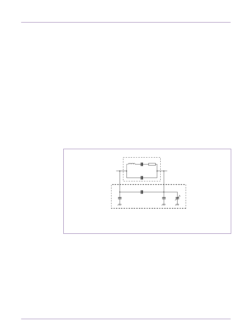
The resonating frequency can be pulled by changing the value of the capacitor at OSCI
or by adding a variable capacitor C
T
at OSCO as shown in Fig 5. External capacitors at
OSCI and OSCO should be connected to GND, except for PCF8573, PCF8583 and
PCF8593. For the latter three it is better to connect these external capacitors to V
DD
instead because these devices are manufactured in a process that has the substrate
connected to V
DD
(n-substrate). In the other RTCs the substrate is at V
SS
(p-substrate).
001aai727
R1
L1
C1
C0
Cstray
Cin
Cout
CT
C
L
crystal
OSCO
OSCI
(1) For PCF8573, PCF8583 and PCF8593 connect C
IN
and C
OUT
(and C
T
if applicable) to V
DD
Fig 5. Oscillator frequency determining components
The reactive components indicated in Fig 4 and Fig 5 determine the oscillating
frequency. Near the resonance frequency the equivalent circuit of the crystal consists of
the motional inductance L
1
, the motional capacitance C
1
and the motional resistance R
1
(in various literature also called series resistance R
S
). In parallel with this series circuit is
the static or shunt capacitance C
0
. It is the sum of the capacitance between the
electrodes and the capacitance added by the leads and mounting structure. If one were
to measure the reactance of the crystal at a frequency far away from a resonance
frequency, it is the reactance of this capacitance that would be measured.
When a crystal is chosen, such a crystal has a specified load capacitance C
L
. During
production the crystal manufacturer has adjusted the resonance frequency of the crystal
using exactly this capacitance as the load for the crystal. The actual value of C
L
as seen
by the crystal in the application is determined by the external circuitry and parasitic
