Nxp semiconductors – NXP Semiconductors UM10301 PCF2123 User Manual
Page 37

NXP Semiconductors
UM10301
User Manual PCF85x3, PCA8565 and PCF2123, PCA2125
UM10301_1
© NXP B.V. 2008. All rights reserved.
User manual
Rev. 01 — 23 December 2008
37 of 52
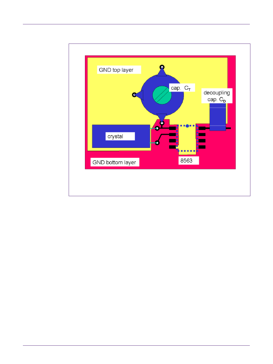
(1) In practice the input capacitor C
T
will in most cases be a fixed capacitor
Fig 14. PCB layout proposal for PCF8563 using leaded components
Alternatively to the last point listed above and in order to achieve highest noise immunity,
a guard ring can be placed around the crystal which must be tied to ground to isolate the
crystal from unwanted noise pickup. It should be tied to V
SS
of the real time clock at one
place only to avoid unforeseen currents running via the guard ring. In addition another
local ground plane on an adjacent PCB layer can be added under the crystal. Also this
ground plane should be isolated from the regular PCB ground plane and connected to
V
SS
of the RTC. The dimensions of this ground plane shouldn’t be much larger than the
perimeter of the guard ring, but optimally should include the complete crystal and RTC.
Be aware that this ground plane will create parasitic capacitances on the OSCI and
OSCO pins because on the adjacent outer layer the tracks to the crystal will run. A
sketch of such a layout is given in Fig 15. Here the use of SMD components is assumed
which is recommended because the smaller dimensions will result in smaller loop area’s.
Both examples use the PCF8563. The same principles apply when one of the other
RTCs is used, with some small modifications due to differences in pinning.
