National Instruments NI 5422 User Manual
Page 17
© National Instruments Corporation
17
NI 5422 Specifications
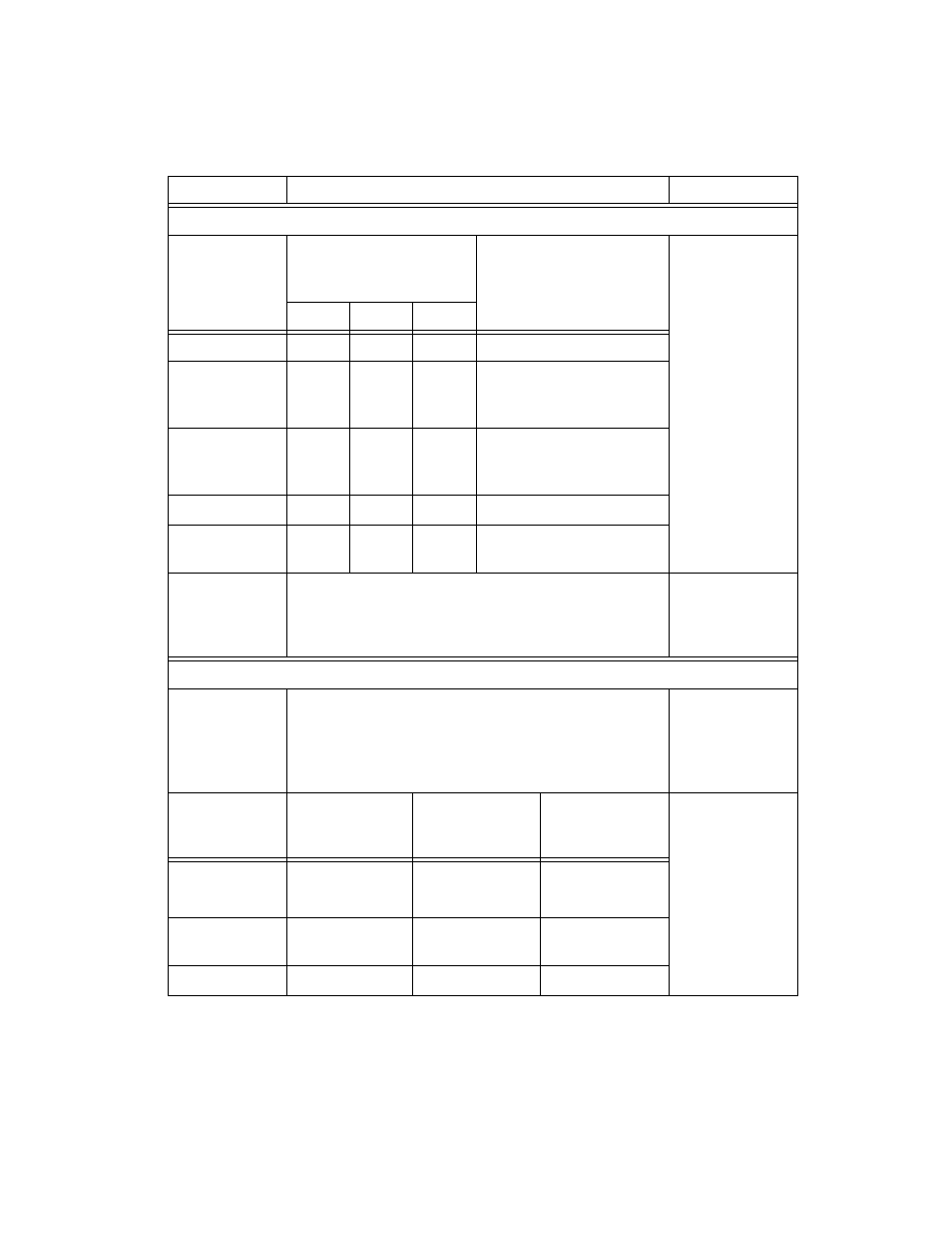
System Phase Noise and Jitter (10 MHz Carrier)
Sample Clock
Source
System Phase Noise
Density
(dBc/Hz) Offset
System Output Jitter
(Integrated from
100 Hz to 100 kHz)
1. High-
Resolution
specifications
vary with
Sample Rate.
2. Values are
typical.
3. PXI Star
trigger
specification is
valid when the
Sample Clock
Source is
locked to
PXI_CLK10.
100 Hz
1 kHz
10 kHz
Divide-by-N
–110
–122
–138
1.5 ps rms
High-
Resolution
1
100 MS/s
–109
–120
–120
4.0 ps rms
High-
Resolution
1
200 MS/s
–108
–120
–122
4.2 ps rms
CLK IN
2
–116
–130
–143
1.1 ps rms
PXI Star
Trigger
2,3
–111
–128
–136
2.1 ps rms
External
Sample Clock
Input Jitter
Tolerance
Cycle-Cycle Jitter ±150 ps
Period Jitter ±1 ns
—
Sample Clock Exporting
Exported
Sample Clock
Destinations
1. PFI<0..1> (SMB front panel connectors)
2. DDC CLK OUT (DIGITAL DATA & CONTROL front
panel connector)
3. PXI_Trig<0..6> (backplane connector)
Exported Sample
Clocks can be
divided by integer
K (1
≤ K ≤
4,194,304).
Exported
Sample Clock
Destinations
Maximum
Frequency
Jitter (Typical)
Duty Cycle
—
PFI<0..1>
200 MHz
PFI 0: 6 ps rms
PFI 1: 12 ps rms
25% to 65%
DDC CLK
OUT
200 MHz
60 ps rms
35% to 65%
PXI_Trig<0..6>
20 MHz
—
—
Table 2. (Continued)
Specification
Value
Comments