Appendix b – cardbus connector information, Connector information, Cardbus connector pinout – Pico Communications E-14 User Manual
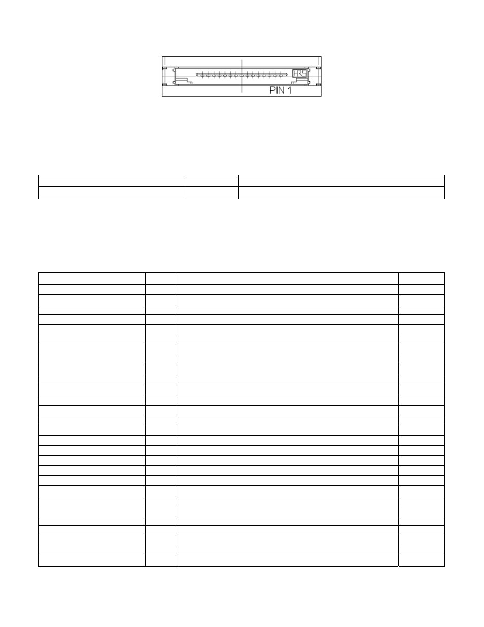
Page 20: Peripheral connector pin #1 location
E‐14 Hardware Reference Manual
www.picocomputing.com
Pico Computing, Inc.
20
Peripheral Connector Pin #1 Location
Figure 5
Appendix B – CardBus Connector Information
Connector Information
Description
Brand
Part Number
CardBus Header
Hirose
IC9‐68RD‐0.635SF‐(51)
The Pico E‐14 will mate with any Type‐II CardBus Header
The function and direction of the pins on the CardBus interface can be easily changed. Please see the
“Digital Bus Interface” section for more information.
CardBus Connector Pinout
Name
Pin
Description
Dir
GND
1
Card Ground
PWR
CAD0
2
CardBus Data/Address 0
IO
CAD1
3
CardBus Data/Address 1
IO
CAD3
4
CardBus Data/Address 3
IO
CAD5
5
CardBus Data/Address 5
IO
CAD7
6
CardBus Data/Address 7
IO
C\C\/\B\E\0\
7
Command and Byte Enable
IO
CAD9
8
CardBus Data/Address 9
IO
CAD11
9
CardBus Data/Address 11
IO
CAD12
10
CardBus Data/Address 12
IO
CAD14
11
CardBus Data/Address 14
IO
C\C\/\B\E\1\
12
Command and Byte Enable
IO
CPAR
13
Parity
IO
C\P\E\R\R\
14
Parity Error
IO
C\G\N\T\
15
Grand
I
C\I\N\T\
16
Card Intert Request
O
VCC
17
Card Power (3.3V)
PWR
VPP
18
Card Programming Voltage (Not Used)
PWR
CCLK
19
CardBus Clock
I
C\I\R\D\Y\
20
Initiator Ready
IO
C\C\/\B\E\2\
21
Command and Byte Enable
IO
CAD18
22
CardBus Data/Address 18
IO
CAD20
23
CardBus Data/Address 20
IO
CAD21
24
CardBus Data/Address 21
IO
CAD22
25
CardBus Data/Address 22
IO
CAD23
26
CardBus Data/Address 23
IO
CAD24
27
CardBus Data/Address 24
IO
CAD25
28
CardBus Data/Address 25
IO