I/o ports, Additional port features – Philips P89LPC903 User Manual
Page 42
Philips Semiconductors
User’s Manual - Preliminary -
P89LPC901/902/903
I/O PORTS
2003 Dec 8
42
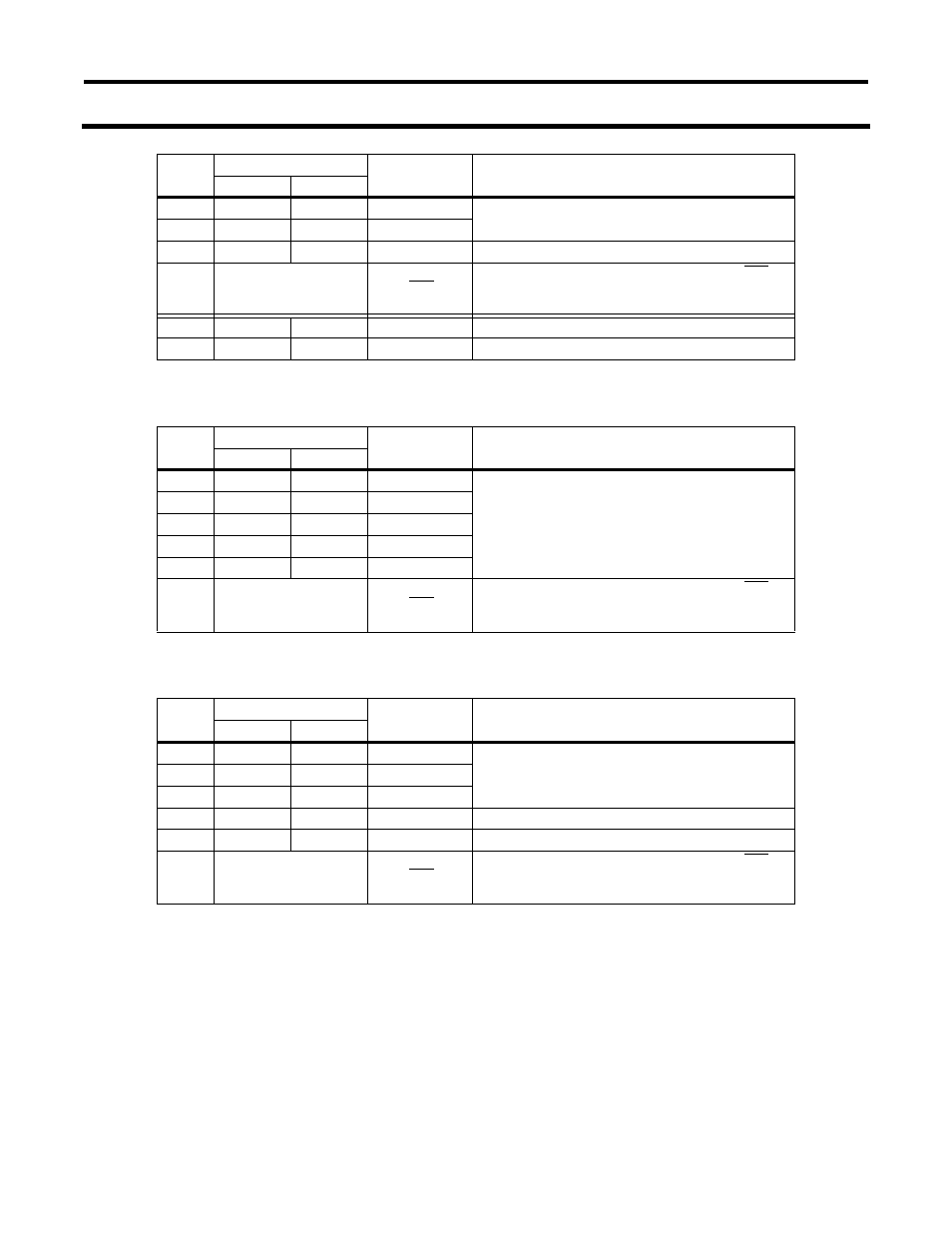
Table 4-3: Port Output Configuration - P89LPC901
Table 4-4: Port Output Configuration - P89LPC902
Table 4-5: Port Output Configuration - P89LPC903
Additional Port Features
After power-up, all pins are in Input-Only mode. Please note that this is different from the LPC76x series of devices.
• After power-up, all I/O pins except P1.5, may be configured by software.
• Pin P1.5 is input only.
• Every output on the P89LPC901/902/903 has been designed to sink typical LED drive current. However, there is a maximum
total output current for all ports which must not be exceeded. Please refer to the P89LPC901/902/903 datasheet for detailed
specifications.
Port
Pin
Configuration SFR Bits
Alternate Usage
Notes
PxM1.y
PxM2.y
P0.4
P0M1.4
P0M2.4
KBI4,CIN1A
Refer to section "Port 0 Analog Functions" for usage as
analog inputs CINxA and CMPREF.
P0.5
P0M1.5
P0M2.5
KBI5,CMPREF
P1.2
P1M1.2
P1M2.2
T0
P1.5
not configurable
RST
Input only. Usage as general purpose input or RST is
determined by User Configuration Bit RPD (UCFG1.6).
Always a reset input during a power-on sequence.
P3.0
P3M1.0
P3M2.0
XTAL2,CLKOUT
P3.1
P3M1.1
P3M2.1
XTAL1
Port
Pin
Configuration SFR Bits
Alternate Usage
Notes
PxM1.y
PxM2.y
P0.0
P0M1.0
P0M2.0
KBI0,CMP2
Refer to section "Port 0 Analog Functions" for usage as
analog inputs CINxA and CMPREF.
P0.2
P0M1.2
P0M2.2
KBI2,CIN2A
P0.4
P0M1.4
P0M2.4
KBI4,CIN1A
P0.5
P0M1.5
P0M2.5
KBI5,CMPREF
P0.6
P0M1.6
P0M2.6
KBI6,CMP1
P1.5
not configurable
RST
Input only. Usage as general purpose input or RST is
determined by User Configuration Bit RPD (UCFG1.6).
Always a reset input during a power-on sequence.
Port
Pin
Configuration SFR Bits
Alternate Usage
Notes
PxM1.y
PxM2.y
P0.2
P0M1.2
P0M2.2
KBI2,CIN2A
Refer to section "Port 0 Analog Functions" for usage as
analog inputs CINxA and CMPREF.
P0.4
P0M1.4
P0M2.4
KBI4,CIN1A
P0.5
P0M1.5
P0M2.5
KBI5,CMPREF
P1.0
P1M1.0
P1M2.0
TxD
P1.1
P1M1.1
P1M2.1
RxD
P1.5
not configurable
RST
Input only. Usage as general purpose input or RST is
determined by User Configuration Bit RPD (UCFG1.6).
Always a reset input during a power-on sequence.