S i 5 3 5 1 a / b / c – Silicon Laboratories SI5351A/B/C User Manual
Page 60
S i 5 3 5 1 A / B / C
60
Preliminary Rev. 0.95
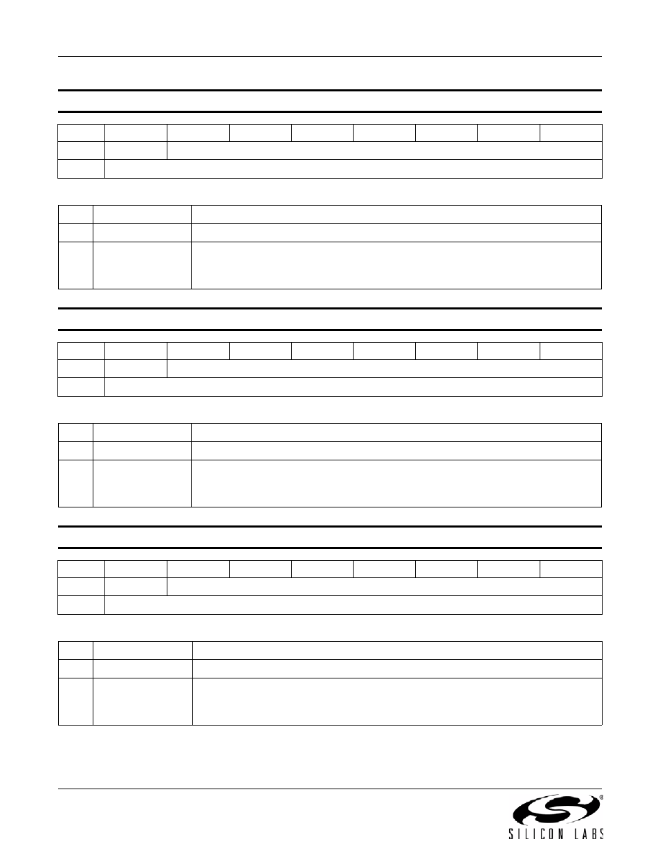
Reset value = 0000 0000
Reset value = 0000 0000
Reset value = 0000 0000
Register 168. CLK3 Initial Phase Offset
Bit
D7
D6
D5
D4
D3
D2
D1
D0
Name
CLK3_PHOFF[6:0]
Type
R/W
R/W
R/W
R/W
R/W
R/W
R/W
R/W
Bit
Name
Function
7
Reserved
Only write 0 to this bit.
6:0
CLK3_PHOFF[6:0] Clock 3 Initial Phase Offset.
CLK3_PHOFF[6:0] is an unsigned integer with one LSB equivalent to a time delay of
Tvco/4, where Tvco is the period of the VCO/PLL associated with this output.
Register 169. CLK4 Initial Phase Offset
Bit
D7
D6
D5
D4
D3
D2
D1
D0
Name
CLK4_PHOFF[6:0]
Type
R/W
R/W
R/W
R/W
R/W
R/W
R/W
R/W
Bit
Name
Function
7
Reserved
Only write 0 to this bit.
6:0
CLK4_PHOFF[6:0] Clock 4 Initial Phase Offset.
CLK4_PHOFF[6:0] is an unsigned integer with one LSB equivalent to a time delay of
Tvco/4, where Tvco is the period of the VCO/PLL associated with this output.
Register 170. CLK5 Initial Phase Offset
Bit
D7
D6
D5
D4
D3
D2
D1
D0
Name
CLK5_PHOFF[6:0]
Type
R/W
R/W
R/W
R/W
R/W
R/W
R/W
R/W
Bit
Name
Function
7
Reserved
Only write 0 to this bit.
6:0
CLK5_PHOFF[6:0] Clock 5 Initial Phase Offset.
CLK5_PHOFF[6:0] is an unsigned integer with one LSB equivalent to a time delay of
Tvco/4, where Tvco is the period of the VCO/PLL associated with this output.