S i 5 3 5 1 a / b / c – Silicon Laboratories SI5351A/B/C User Manual
Page 28
S i 5 3 5 1 A / B / C
28
Preliminary Rev. 0.95
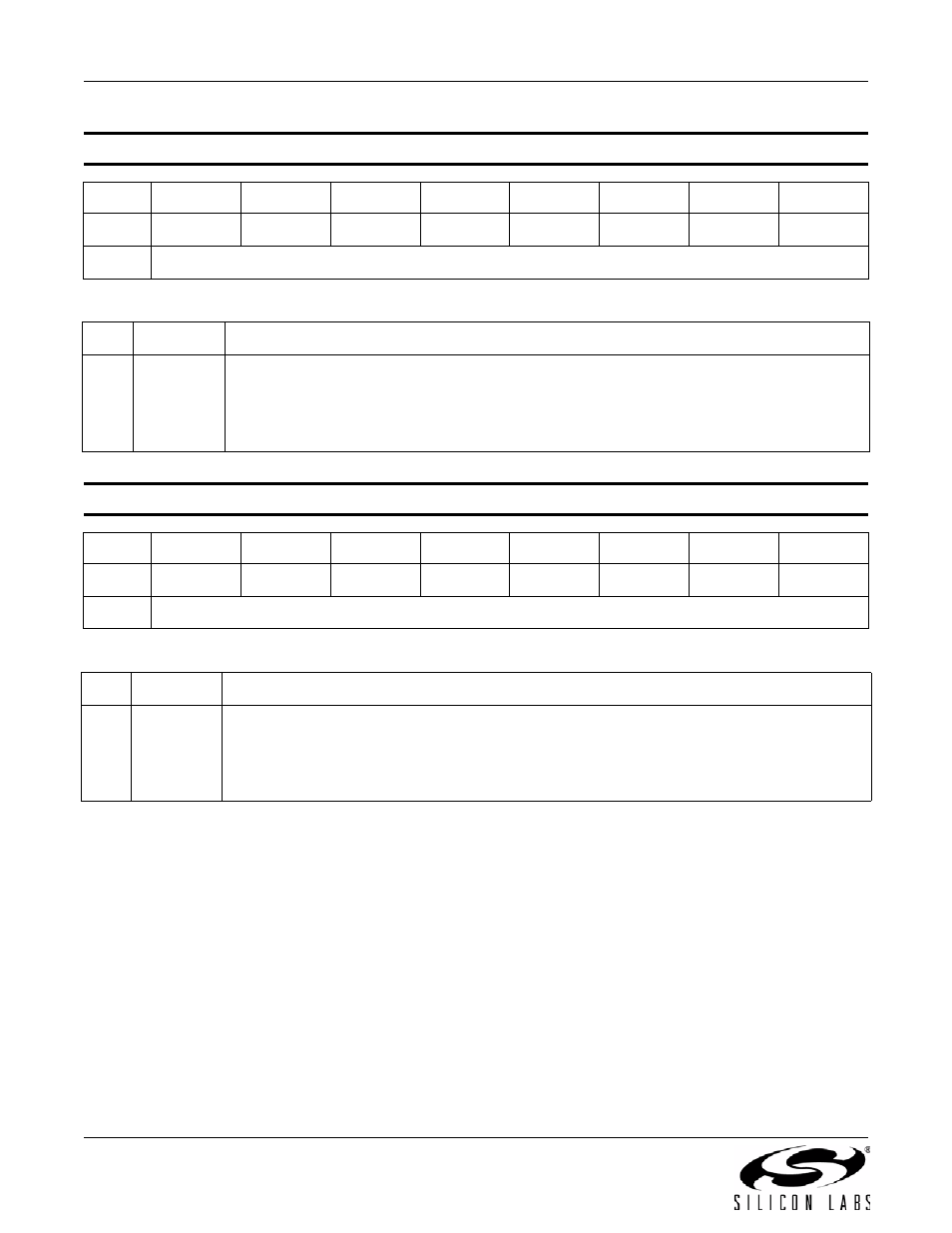
Reset value = 0000 0000
Reset value = 0000 0000
Register 3. Output Enable Control
Bit
D7
D6
D5
D4
D3
D2
D1
D0
Name
CLK7_OEB CLK6_OEB CLK5_OEB CLK4_OEB CLK3_OEB CLK2_OEB CLK1_OEB CLK0_OEB
Type
R/W
R/W
R/W
R/W
R/W
R/W
R/W
R/W
Bit
Name
Function
7:0
CLKx_OEB Output Disable for CLKx.
Where x = 0, 1, 2, 3, 4, 5, 6, 7
0: Enable CLKx output.
1: Disable CLKx output.
Register 9. OEB Pin Enable Control
Bit
D7
D6
D5
D4
D3
D2
D1
D0
Name
OEB_CLK7 OEB_CLK6 OEB_CLK5 OEB_CLK4 OEB_CLK3 OEB_CLK2 OEB_CLK1 OEB_CLK0
Type
R/W
R/W
R/W
R/W
R/W
R/W
R/W
R/W
Bit
Name
Function
7:0
OEB_CLKx OEB pin enable control of CLKx.
Where x = 0, 1, 2, 3, 4, 5, 6, 7
0: OEB pin controls enable/disable state of CLKx output.
1: OEB pin does not control enable/disable state of CLKx output.