Hardware information, Block diagram, Block diagram technical data – Spectrum Brands MC.31XX User Manual
Page 12
12
MC.31xx Manual
Hardware information
Introduction
Hardware information
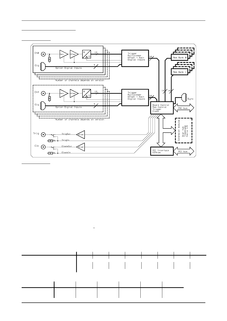
Block diagram
Technical Data
Resolution
12 bit
Dimension
160 x 233 mm (Standard 6U)
Differential linearity error
≤ 1 LSB (ADC)
Width (Standard)
1 slot
Integral linearity error
≤ 2.5 LSB (ADC)
Width (with digital inputs)
2 slots
Multi: Trigger to 1st sample delay
fix
Connector
3 mm SMB male
Multi: Recovery time
< 20 samples
Input impedance
50 Ohm / 1 MOhm || 25 pF
ext. Trigger accuracy
1 Samples
Overvoltage protection (range ≤ ±1 V)
±5 V
int. Trigger accuracy
1 Sample
Overvoltage protection (range > ±1 V)
±50 V
Ext. clock: delay to internal clock
42 ns ±2 ns
Warm up time
10 minutes
input signal with 50 ohm termination
max 5 V rms
Operating temperature
0°C - 50°C
Digital Inputs input impedance
110 Ohm @ 2.5 V
Storage temperature
-10°C - 70°C
Digital Inputs delay to analog sample
-4 samples
Humidity
10% to 90%
Min internal clock
1 kS/s
Min external clock
1 kS/s
Power consumption 5 V @ full speed
max. 3.3 A (16.5 Watt)
Power consumption 5 V @ power down
max. 2.5 A (12.5 Watt)
Trigger input:Standard TTL level
Low: -0.5 > level < 0.8 V
High: 2.0 V > level < 5.5 V
Trigger pulse must be valid > 2 clock periods.
Clock input: Standard TTL level
Low: -0.5 V > level < 0.8 V
High: 2.0 V > level < 5.5 V
Rising edge. Duty cycle: 50% ± 5%
Trigger output
Standard TTL, capable of driving 50 Ohm.
Low < 0.4 V (@ 20 mA, max 64 mA)
High > 2.4 V (@ -20 mA, max -48 mA)
One positive edge after the first internal trigger
Clock output
Standard TTL, capable of driving 50 Ohm
Low < 0.4 V (@ 20 mA, max 64 mA)
High > 2.4 V (@ -20 mA, max -48 mA)
Input range
±50 mV
±100 mV
±200 mV
±500 mV
±1 V
±2 V
±5 V
±10 V
Software programmable offset
±50 mV
±100 mV
±200 mV
±500 mV
±1 V
±2 V
±5 V
±10 V
Offset error
< 1 LSB, adjustable by user
Gain error
< 1 %
< 1 %
< 1 %
< 1 %
< 1 %
< 1 %
< 1 %
< 1 %
Noise (rms): 50 Ohm, 25 MS/s
< 1.5 LSB
< 1.2 LSB
< 1.0 LSB
< 1.0 LSB
< 1.0 LSB
< 1.0 LSB
< 1.0 LSB
< 1.0 LSB
Crosstalk 500 kHz signal, ±50 mV input, 50 Ohm
< -70 dB
MC.3110
MC.3111
MC.3112
MC.3120
MC.3121
MC.3122
MC.3130
MC.3131
MC.3132
max internal clock
1 MS/s
1 MS/s
10 MS/s
10 MS/s
25 MS/s
25 MS/s
max external clock
1 MS/s
1 MS/s
10 MS/s
10 MS/s
25 MS/s
25 MS/s
-3 dB bandwidth
> 500 kHz
> 500 kHz
> 5 MHz
> 5 MHz
> 12.5 MHz
> 12.5 MHz