Chapter 6 pin descriptions, Datasheet – SMSC USB97C242 User Manual
Page 12
USB 2.0 Flash Drive Controller
Datasheet
SMSC USB97C242
Page 12
Revision 1.4 (05-03-07)
DATASHEET
Chapter 6 Pin Descriptions
This section provides a detailed description of each signal. The signals are arranged in functional groups
according to their associated interface.
The “n” symbol in the signal name indicates that the active, or asserted state occurs when the signal is at a
low voltage level. When “n” is not present before the signal name, the signal is asserted when at the high
voltage level.
The terms assertion and negation are used exclusively. This is done to avoid confusion when working with
a mixture of “active low” and “active high” signal. The term assert, or assertion indicates that a signal is
active, independent of whether that level is represented by a high or low voltage. The term negate, or
negation indicates that a signal is inactive.
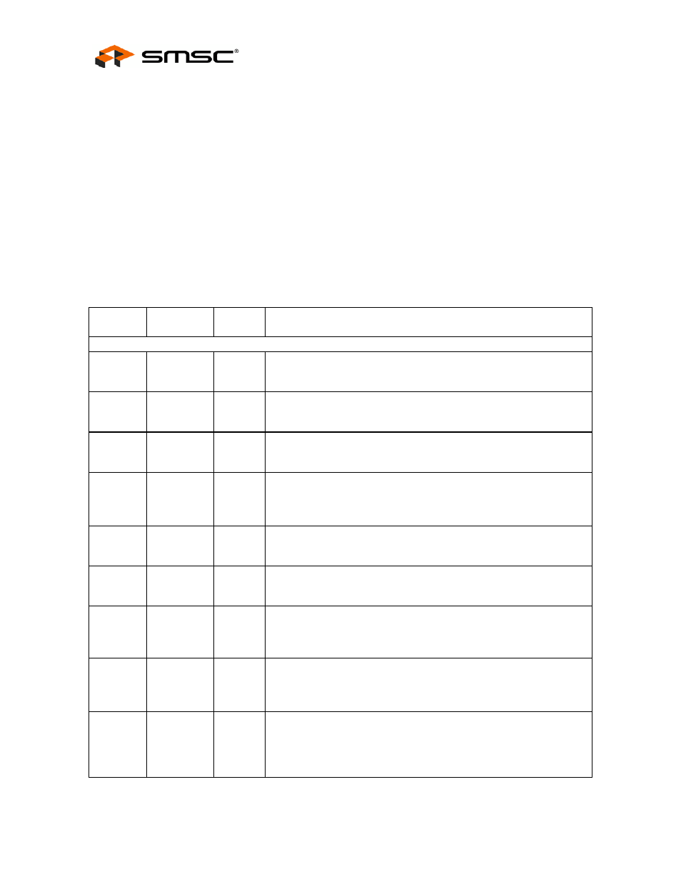
Table 6.1 – USB97C242 Pin Descriptions
NAME
SYMBOL
BUFFER
TYPE
DESCRIPTION
NAND FLASH/SMARTMEDIA INTERFACE
SM
Write
Protect
nWP
O12
This pin is an active low write protect signal for the SM or NAND flash
device.
SM
Address
Strobe
ALE
O12
This pin is an active high Address Latch Enable signal for the SM or
NAND flash device.
SM
Command
Strobe
CLE
O12
This pin is an active high Command Latch Enable signal for the SM or
NAND flash device.
SM
Data7-0
D[7:0]
I/OPU12 These pins are the bi-directional data signal D7-D0.
The bi-directional input signal should have an internal weak pull-up
resister on the input.
SM
Read
Enable
nRE
O24
This pin is an active low read strobe signal for SM or NAND flash device.
SM
Write
Enable
nWE
O12
This pin is an active low write strobe signal for SM or NAND flash device.
SM
Write
Protect
Switch
nWPS
IPU
A write-protect seal is detected, when this pin is low.
This pin has an internal weak pull-up resistor.
SM
Busy or
Data Ready
nB/R
IPU
This pin is connected to the BSY/RDY pin of the SM or NAND flash
device.
This pin has an internal weak pull-up resistor.
SM
Chip
Enable
nCE
OPU8
This pin is the active low chip enable signal to the SM or NAND flash
device.
This pin should be used to support a single SM or NAND flash device
only.