0 electrical specifications and timing parameters, 1 absolute maximum ratings, 2 general operating conditions – Intel 82555 User Manual
Page 47: 3 dc characteristics, 1 mii dc characteristics, 2 10base-t voltage/current dc characteristics, Electrical specifications and timing parameters, Absolute maximum ratings, General operating conditions, Dc characteristics
Datasheet
43
Networking Silicon — 82555
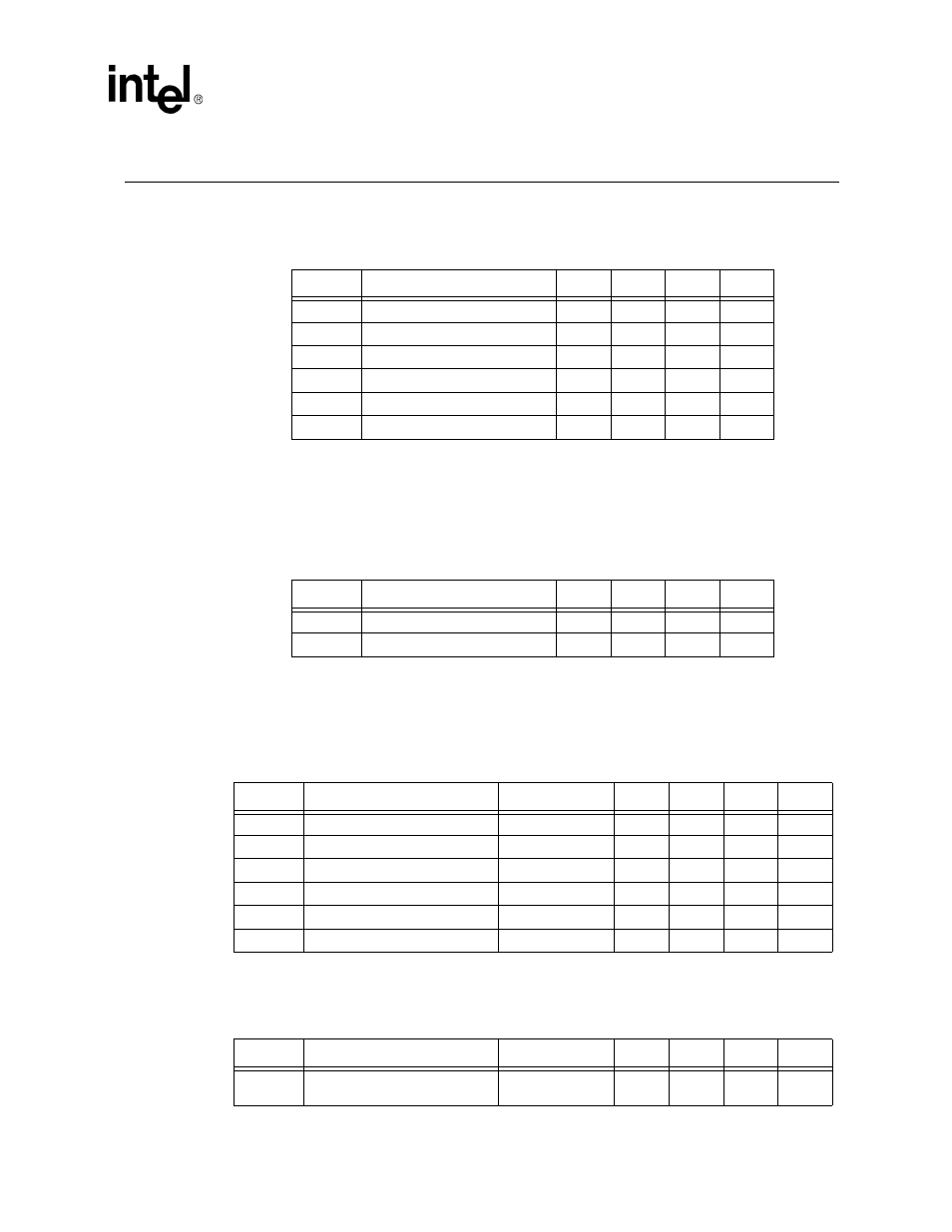
11.0
Electrical Specifications and Timing Parameters
11.1
Absolute Maximum Ratings
11.2
General Operating Conditions
11.3
DC Characteristics
11.3.1
MII DC Characteristics
11.3.2
10BASE-T Voltage/Current DC Characteristics
Symbol
Parameter Description
Min
Typ
Max
Units
T
C
Case temperature under bias
0
85
C
T
S
Storage temperature
-65
140
C
V
SUP
Supply voltage
-0.5
7.0
V
V
OA
a
a. Stresses above the listed under absolute maximum ratings may cause permanent damage to the
device. This is a stress rating only and functional operations of the device at these or any other
conditions above those indicated in the operational sections of this specification is not implied. Ex-
posure to absolute maximum rating conditions for extended periods may affect device reliability.
All output voltages
-0.5
7.0
V
V
OTD
Transmit Data Output Voltage
-0.5
8.0
V
V
IA
All input voltages
-1.0
6.0
V
Symbol
Parameter Description
Min
Typ
Max
Units
V
CC
Supply voltage
4.75
5.25
V
T
C
Case temperature
0
85
C
Symbol
Parameter Description
Condition
Min
Typ
Max
Units
V
IL
Input low voltage (TTL)
0
0.8
V
V
IH
Input high voltage (TTL)
2.0
V
V
OL
Output low voltage
I
out
= 4 mA
0.45
V
V
OH
Output high voltage
I
out
= -4 mA
2.4
V
I
IL
Input low leakage current
0 < V
in
< V
CC
±15
µ
A
C
IN
a
a. This parameter is only characterized, not tested. It is valid for digital pins only.
Input capacitance
10
pF
Symbol
Parameter Description
Condition
Min
Typ
Max
Units
R
ID10
a
Input differential resistance
DC and V
RDP
=
(V
CC
/2) + 0.5 V
10
K
Ω