Typical operating characteristics, Electrical characteristics (continued) – Maxim Integrated MAX12557 User Manual
Page 7
MAX12557
Dual, 65Msps, 14-Bit, IF/Baseband ADC
_______________________________________________________________________________________
7
ELECTRICAL CHARACTERISTICS (continued)
(V
DD
= 3.3V, OV
DD
= 2.0V, GND = 0, REFIN = REFOUT (internal reference), C
L
≈ 10pF at digital outputs, V
IN
= -0.5dBFS (differen-
tial), DIFFCLK/SECLK = OV
DD
, PD = GND, SHREF = GND, DIV2 = GND, DIV4 = GND, G/T = GND, f
CLK
= 65MHz, T
A
= -40°C to
+85°C, unless otherwise noted. Typical values are at T
A
= +25°C.) (Note 1)
PARAMETER
SYMBOL
CONDITIONS
MIN
TYP
MAX
UNITS
TIMING CHARACTERISTICS (Figure 5)
Clock Pulse-Width High
t
CH
7.7
ns
Clock Pulse-Width Low
t
CL
7.7
ns
Data-Valid Delay
t
DAV
5.4
ns
Data Setup Time Before Rising
Edge of DAV
t
SETUP
(Note 6)
7.0
ns
Data Hold Time After Rising Edge
of DAV
t
HOLD
(Note 6)
7.0
ns
Wake-Up Time from Power-Down
t
WAKE
V
REFIN
= 2.048V
10
ms
Note 1: Specifications
≥+25°C guaranteed by production test, <+25°C guaranteed by design and characterization.
Note 2: Guaranteed by design and characterization. Device tested for performance during product test.
Note 3: Specification guaranteed by production test for
≥+25°C.
Note 4: Two-tone intermodulation distortion measured with respect to a single-carrier amplitude, and not the peak-to-average input
power of both input tones.
Note 5: During power-down, D0A–D13A, D0B–D13B, DORA, DORB, and DAV are high impedance.
Note 6: Guaranteed by design and characterization.
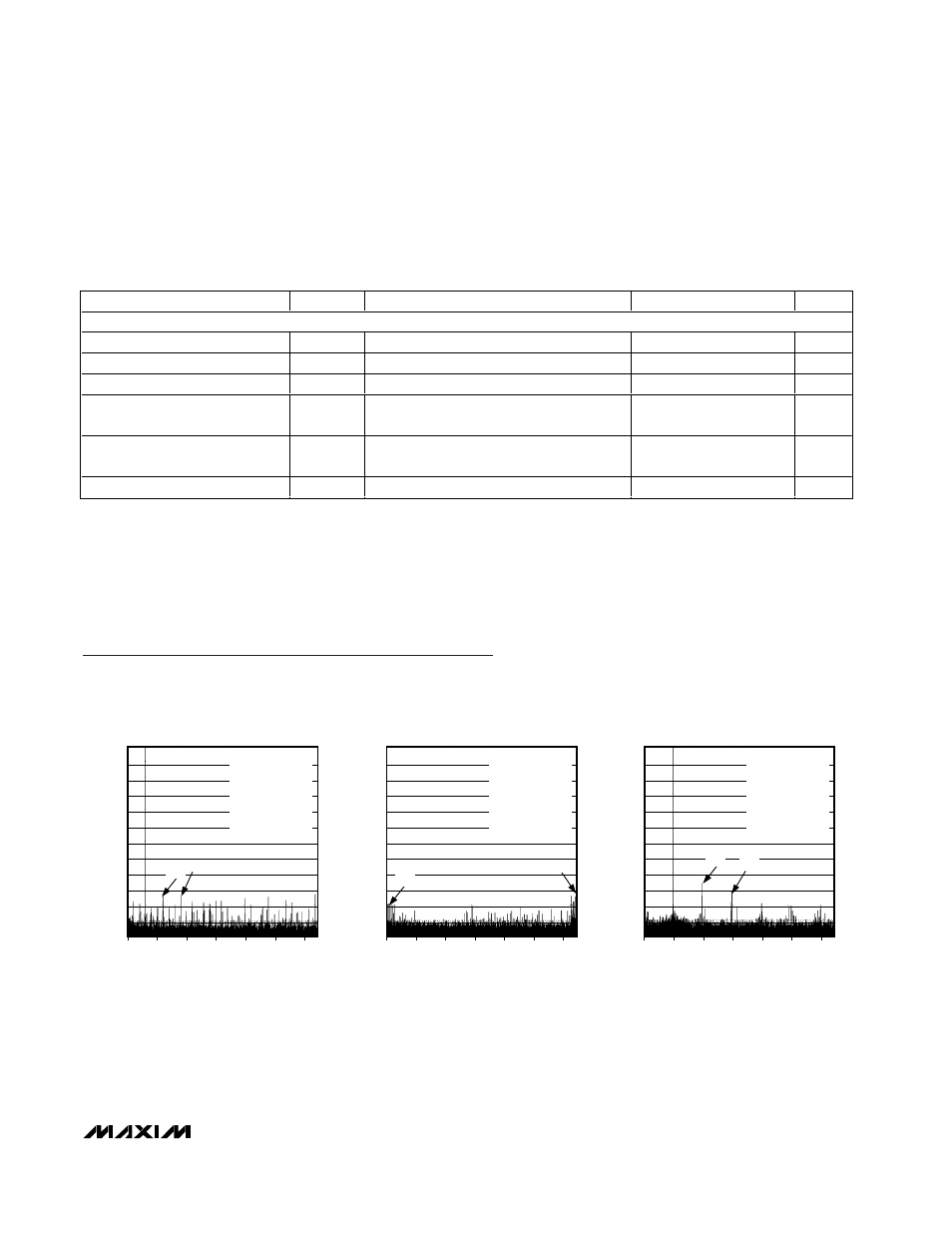
Typical Operating Characteristics
(V
DD
= 3.3V, OV
DD
= 2.0V, GND = 0, REFIN = REFOUT (internal reference mode), C
L
≈ 5pF at digital outputs, V
IN
= -0.5dBFS,
DIFFCLK/SECLK = OV
DD
, PD = GND, G/T = GND, f
CLK
= 65MHz (50% duty cycle), T
A
= +25°C, unless otherwise noted.)
FFT PLOT (32,768-POINT DATA RECORD)
MAX12557 toc01
ANALOG INPUT FREQUENCY (MHz)
AMPLITUDE (dBFS)
-100
-80
-60
-40
-20
0
-120
HD3
f
CLK
= 65MHz
f
IN
= 3.00125MHz
A
IN
= -0.48dBFS
SNR = 74.45dB
SINAD = 74.33dB
THD = -90.06dBc
SFDR = 92.47dBc
HD2
-10
-30
-50
-70
-90
-110
30
25
15
20
10
5
0
FFT PLOT (32,768-POINT DATA RECORD)
MAX12557 toc02
ANALOG INPUT FREQUENCY (MHz)
AMPLITUDE (dBFS)
-100
-80
-60
-40
-20
0
-120
HD3
f
CLK
= 65.00352MHz
f
IN
= 32.40058MHz
A
IN
= -0.424dBFS
SNR = 74.77dB
SINAD = 74.62dB
THD = -87.22dBc
SFDR = 91.88dBc
HD2
-10
-30
-50
-70
-90
-110
30
25
15
20
10
5
0
FFT PLOT (32,768-POINT DATA RECORD)
MAX12557 toc03
ANALOG INPUT FREQUENCY (MHz)
AMPLITUDE (dBFS)
-100
-80
-60
-40
-20
0
-120
f
CLK
= 65.00352MHz
f
IN
= 70.00852MHz
A
IN
= -0.498dBFS
SNR = 74.41dB
SINAD = 74.00dB
THD = -84.50dBc
SFDR = 86.25dBc
HD2
-10
-30
-50
-70
-90
-110
HD3
30
25
15
20
10
5
0