Maxim Integrated MAX12557 User Manual
Page 2
MAX12557
Dual, 65Msps, 14-Bit, IF/Baseband ADC
2
_______________________________________________________________________________________
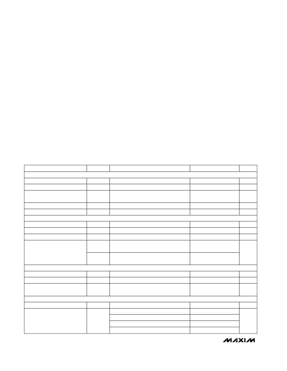
ABSOLUTE MAXIMUM RATINGS
ELECTRICAL CHARACTERISTICS
(V
DD
= 3.3V, OV
DD
= 2.0V, GND = 0, REFIN = REFOUT (internal reference), C
L
≈ 10pF at digital outputs, V
IN
= -0.5dBFS (differen-
tial), DIFFCLK/
SECLK = OV
DD
, PD = GND, SHREF = GND, DIV2 = GND, DIV4 = GND, G/T = GND, f
CLK
= 65MHz, T
A
= -40°C to
+85°C, unless otherwise noted. Typical values are at T
A
= +25°C.) (Note 1)
Stresses beyond those listed under “Absolute Maximum Ratings” may cause permanent damage to the device. These are stress ratings only, and functional
operation of the device at these or any other conditions beyond those indicated in the operational sections of the specifications is not implied. Exposure to
absolute maximum rating conditions for extended periods may affect device reliability.
V
DD
to GND ................................................................-0.3V to +3.6V
OV
DD
to GND............-0.3V to the lower of (V
DD
+ 0.3V) and +3.6V
INAP, INAN to GND ...-0.3V to the lower of (V
DD
+ 0.3V) and +3.6V
INBP, INBN to GND ...-0.3V to the lower of (V
DD
+ 0.3V) and +3.6V
CLKP, CLKN to
GND ........................-0.3V to the lower of (V
DD
+ 0.3V) and +3.6V
REFIN, REFOUT
to GND ..................-0.3V to the lower of (V
DD
+ 0.3V) and +3.6V
REFAP, REFAN,
COMA to GND ......-0.3V to the lower of (V
DD
+ 0.3V) and +3.6V
REFBP, REFBN,
COMB to GND ......-0.3V to the lower of (V
DD
+ 0.3V) and +3.6V
DIFFCLK/SECLK, G/T, PD, SHREF, DIV2,
DIV4 to GND .........-0.3V to the lower of (V
DD
+ 0.3V) and +3.6V
D0A–D13A, D0B–D13B, DAV,
DORA, DORB to GND..............................-0.3V to (OV
DD
+ 0.3V)
Continuous Power Dissipation (T
A
= +70°C)
68-Pin Thin QFN 10mm x 10mm x 0.8mm
(derate 70mW/°C above +70°C) ....................................4000mW
Operating Temperature Range................................-40°C to +85°C
Junction Temperature ...........................................................+150°C
Storage Temperature Range .................................-65°C to +150°C
Lead Temperature (soldering 10s).......................................+300°C
PARAMETER
SYMBOL
CONDITIONS
MIN
TYP
MAX
UNITS
DC ACCURACY
Resolution
14
Bits
Integral Nonlinearity
INL
f
IN
= 3MHz
±2.1
LSB
Differential Nonlinearity
DNL
f
IN
= 3MHz, no missing codes over
temperature (Note 2)
-1.0
±0.6
+1.3
LSB
Offset Error
±0.1
±0.9
%FSR
Gain Error
±0.5
±5.0
%FSR
ANALOG INPUT (INAP, INAN, INBP, INBN)
Differential Input Voltage Range
V
DIFF
Differential or single-ended inputs
±1.024
V
Common-Mode Input Voltage
V
DD
/ 2
V
Analog Input Resistance
R
IN
Each input, Figure 3
3.4
k
Ω
C
PAR
Fixed capacitance to ground,
each input, Figure 3
2
Analog Input Capacitance
C
SAMPLE
Switched capacitance,
each input, Figure 3
4.5
pF
CONVERSION RATE
Maximum Clock Frequency
f
CLK
65
MHz
Minimum Clock Frequency
5
MHz
Data Latency
Figure 5
8
Clock
Cycles
DYNAMIC CHARACTERISTICS (differential inputs)
Small-Signal Noise Floor
SSNF
Input at -35dBFS
74.5
76
dBFS
f
IN
= 3MHz at -0.5dBFS
72.5
75
f
IN
= 32.5MHz at -0.5dBFS
74.5
f
IN
= 70MHz at -0.5dBFS
74.1
Signal-to-Noise Ratio
SNR
f
IN
= 175MHz at -0.5dBFS
70.4
72.5
dB