Electrical characteristics (continued) – Maxim Integrated MAX12557 User Manual
Page 6
MAX12557
Dual, 65Msps, 14-Bit, IF/Baseband ADC
6
_______________________________________________________________________________________
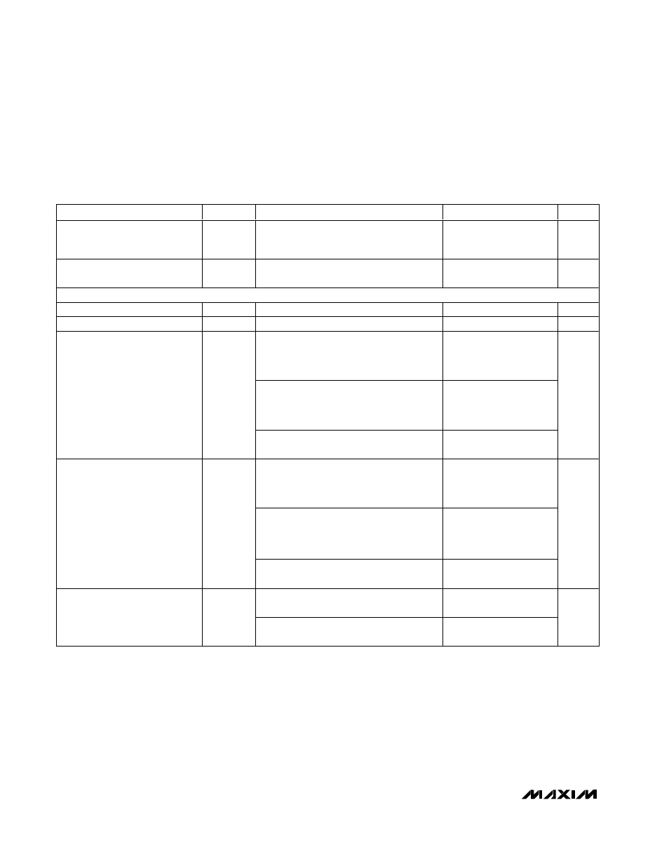
ELECTRICAL CHARACTERISTICS (continued)
(V
DD
= 3.3V, OV
DD
= 2.0V, GND = 0, REFIN = REFOUT (internal reference), C
L
≈ 10pF at digital outputs, V
IN
= -0.5dBFS (differen-
tial), DIFFCLK/SECLK = OV
DD
, PD = GND, SHREF = GND, DIV2 = GND, DIV4 = GND, G/T = GND, f
CLK
= 65MHz, T
A
= -40°C to
+85°C, unless otherwise noted. Typical values are at T
A
= +25°C.) (Note 1)
PARAMETER
SYMBOL
CONDITIONS
MIN
TYP
MAX
UNITS
D 0A–D 13A, D O RA,
D 0B–D 13B and D ORB Tr i - S tate
O utp ut C ap aci tance ( N ote 3)
C
OUT
3
pF
DAV Tri-State Output
Capacitance (Note 3)
C
DAV
6
pF
POWER REQUIREMENTS
Analog Supply Voltage
V
DD
3.15
3.30
3.60
V
Digital Output Supply Voltage
OV
DD
1.70
2.0
V
DD
V
Normal operating mode
f
IN
= 175MHz at -0.5dBFS,
single-ended clock
(DIFFCLK/SECLK = GND)
185
Normal operating mode
f
IN
= 175MHz at -0.5dBFS
differential clock
(DIFFCLK/SECLK = OV
DD
)
193
210
Analog Supply Current
I
VDD
Power-down mode (PD = OV
DD
)
clock idle
0.05
mA
Normal operating mode
f
IN
= 175MHz at -0.5dBFS
single-ended clock
(DIFFCLK/SECLK = GND)
610
Normal operating mode
f
IN
= 175MHz at -0.5dBFS
differential clock
(DIFFCLK/SECLK = OV
DD
)
637
693
Analog Power Dissipation
P
VDD
Power-down mode (PD = OV
DD
)
clock idle
0.165
mW
Normal operating mode
f
IN
= 175MHz at -0.5dBFS
21.3
Digital Output Supply Current
I
OVDD
Power-down mode (PD = OV
DD
)
clock idle
0.001
mA