Dual, 65msps, 14-bit, if/baseband adc, Detailed description, Pin description (continued) – Maxim Integrated MAX12557 User Manual
Page 14
MAX12557
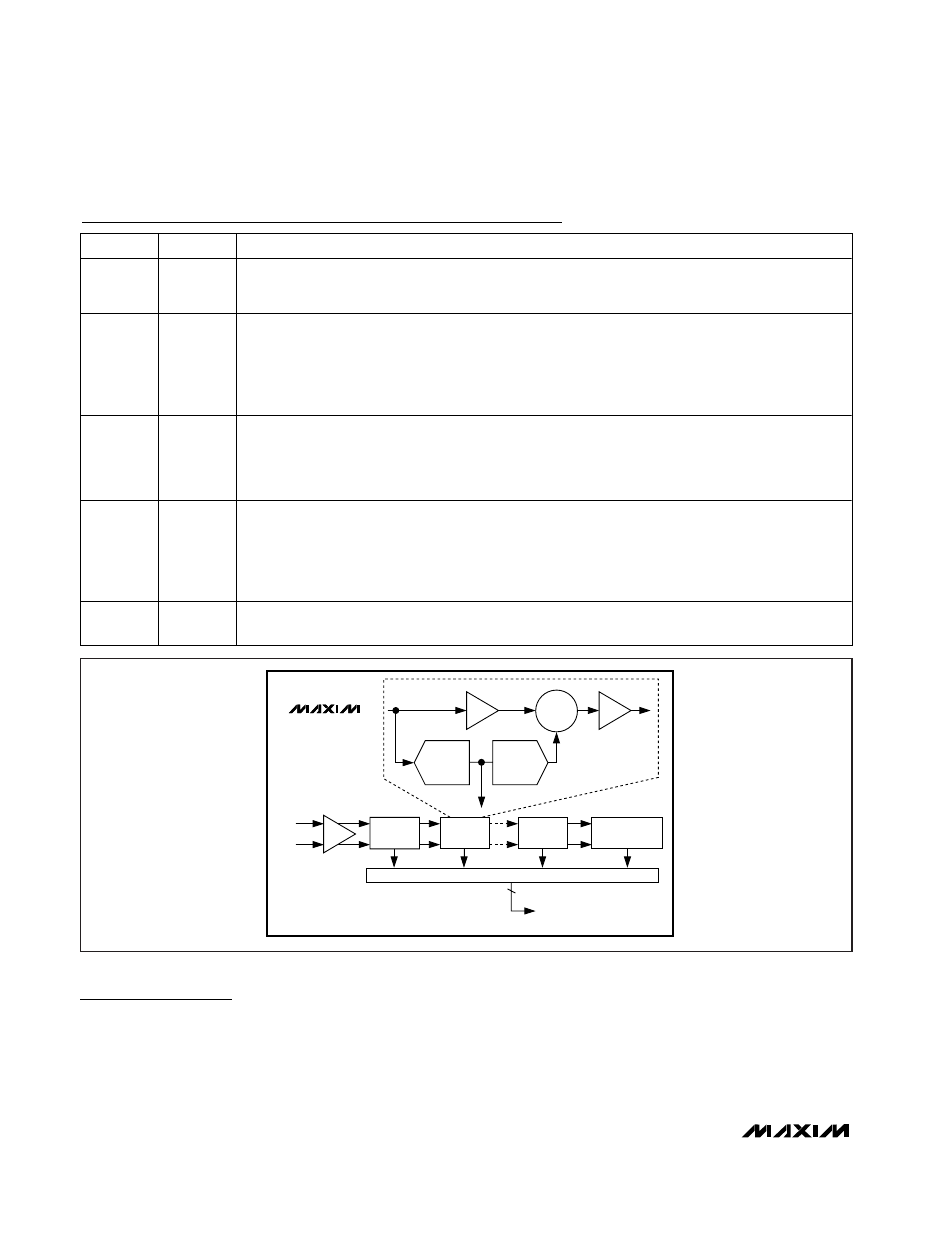
Detailed Description
The MAX12557 uses a 10-stage, fully differential,
pipelined architecture (Figure 1) that allows for high-
speed conversion while minimizing power consump-
tion. Samples taken at the inputs move progressively
through the pipeline stages every half clock cycle.
From input to output the total latency is 8 clock cycles.
Each pipeline converter stage converts its input voltage
to a digital output code. At every stage, except the last,
the error between the input voltage and the digital out-
put code is multiplied and passed along to the next
pipeline stage. Digital error correction compensates for
ADC comparator offsets in each pipeline stage and
ensures no missing codes. Figure 2 shows the
MAX12557 functional diagram.
Dual, 65Msps, 14-Bit, IF/Baseband ADC
14
______________________________________________________________________________________
PIN
NAME
FUNCTION
65
PD
Power-Down Digital Input.
PD = GND: ADCs are fully operational.
PD = OV
DD
: ADCs are powered down.
66
SHREF
Shared Reference Digital Input.
SHREF = V
DD
: Shared reference enabled.
SHREF = GND: Shared reference disabled.
When sharing the reference, externally connect REFAP and REFBP together to ensure that V
REFAP
=
V
REFBP
. Similarly, when sharing the reference, externally connect REFAN to REFBN together to ensure
that V
REFAN
= V
REFBN
.
67
REFOUT
Inter nal Refer ence V ol tag e O utp ut. The RE FOU T outp ut vol tag e i s 2.048V and RE FO U T can d el i ver 1m A.
For internal reference operation, connect REFOUT directly to REFIN or use a resistive divider from
REFOUT to set the voltage at REFIN. Bypass REFOUT to GND with a
≥0.1µF capacitor.
For external reference operation, REFOUT is not required and must be bypassed to GND with a
≥0.1µF
capacitor.
68
REFIN
Single-Ended Reference Analog Input.
For i nter nal r efer ence and b uffer ed exter nal r efer ence op er ati on, ap p l y a 0.7V to 2.3V D C r efer ence
vol tag e to RE FIN . B y p a s s REF I N t o GN D w it h a 4 . 7 µ F c a p a c i t o r . W i thi n i ts sp eci fi ed op er ati ng vol tag e,
RE FIN has a > 50M
Ω i np ut i m p ed ance, and the d i ffer enti al r efer ence vol tag e ( V
R E F_ P
- V
R E F_ N
) i s
g ener ated fr om RE FIN . For unb uffer ed exter nal r efer ence op er ati on, connect RE FIN to G N D . In thi s
m od e, RE F_P , RE F_N , and C O M _ ar e hi g h- i m p ed ance i np uts that accep t the exter nal r efer ence vol tag es.
—
EP
Exposed Paddle. EP is internally connected to GND. Externally connect EP to GND to achieve specified
dynamic performance.
Pin Description (continued)
MAX12557
Σ
+
−
DIGITAL ERROR CORRECTION
FLASH
ADC
x2
DAC
STAGE 2
IN_P
IN_N
STAGE 1
STAGE 9
STAGE 10
END OF PIPELINE
D0_ THROUGH D13_
Figure 1. Pipeline Architecture—Stage Blocks