Dual, 65msps, 14-bit, if/baseband adc – Maxim Integrated MAX12557 User Manual
Page 20
MAX12557
The digital outputs D0A/B–D13A/B are high impedance
when the MAX12557 is in power-down (PD = 1) mode.
D0A/B–D13A/B enter this state 10ns after the rising
edge of PD and become active again 10ns after PD
transitions low.
Keep the capacitive load on the MAX12557 digital out-
puts D0A/B–D13A/B as low as possible (<15pF) to
avoid large digital currents feeding back into the ana-
log portion of the MAX12557 and degrading its dynam-
ic performance. Adding external digital buffers on the
digital outputs helps isolate the MAX12557 from heavy
capacitive loads. To improve the dynamic performance
of the MAX12557, add 220
Ω resistors in series with the
digital outputs close to the MAX12557. Refer to the
MAX12557 EV kit schematic for guidelines of how to
drive the digital outputs through 220
Ω series resistors
and external digital output buffers.
Power-Down Input
The MAX12557 has two power modes that are con-
trolled with a power-down digital input (PD). With PD
low, the MAX12557 is in its normal operating mode.
With PD high, the MAX12557 is in power-down mode.
The power-down mode allows the MAX12557 to effi-
ciently use power by transitioning to a low-power state
when conversions are not required. Additionally, the
MAX12557 parallel output bus goes high-impedance in
power-down mode, allowing other devices on the bus
to be accessed.
In power-down mode all internal circuits are off, the
analog supply current reduces to less than 50µA, and
the digital supply current reduces to 1µA. The following
list shows the state of the analog inputs and digital out-
puts in power-down mode.
1) INAP/B, INAN/B analog inputs are disconnected
from the internal input amplifier (Figure 3).
2) REFOUT has approximately 17k
Ω to GND.
3) REFAP/B, COMA/B, REFAN/B enter a high-imped-
ance state with respect to V
DD
and GND, but there
is an internal 4k
Ω resistor between REFAP/B and
COMA/B as well as an internal 4k
Ω resistor
between REFAN/B and COMA/B.
4) D0A–D13A, D0B–D13B, DORA, and DORB enter a
high-impedance state.
5) DAV enters a high-impedance state.
6) CLKP, CLKN clock inputs enter a high-impedance
state (Figure 4).
The wake-up time from power-down mode is dominated
by the time required to charge the capacitors at REF_P,
REF_N, and COM_. In internal reference mode and
buffered external reference mode the wake-up time is
typically 10ms. When operating in the unbuffered exter-
nal reference mode the wake-up time is dependent on
the external reference drivers.
Dual, 65Msps, 14-Bit, IF/Baseband ADC
20
______________________________________________________________________________________
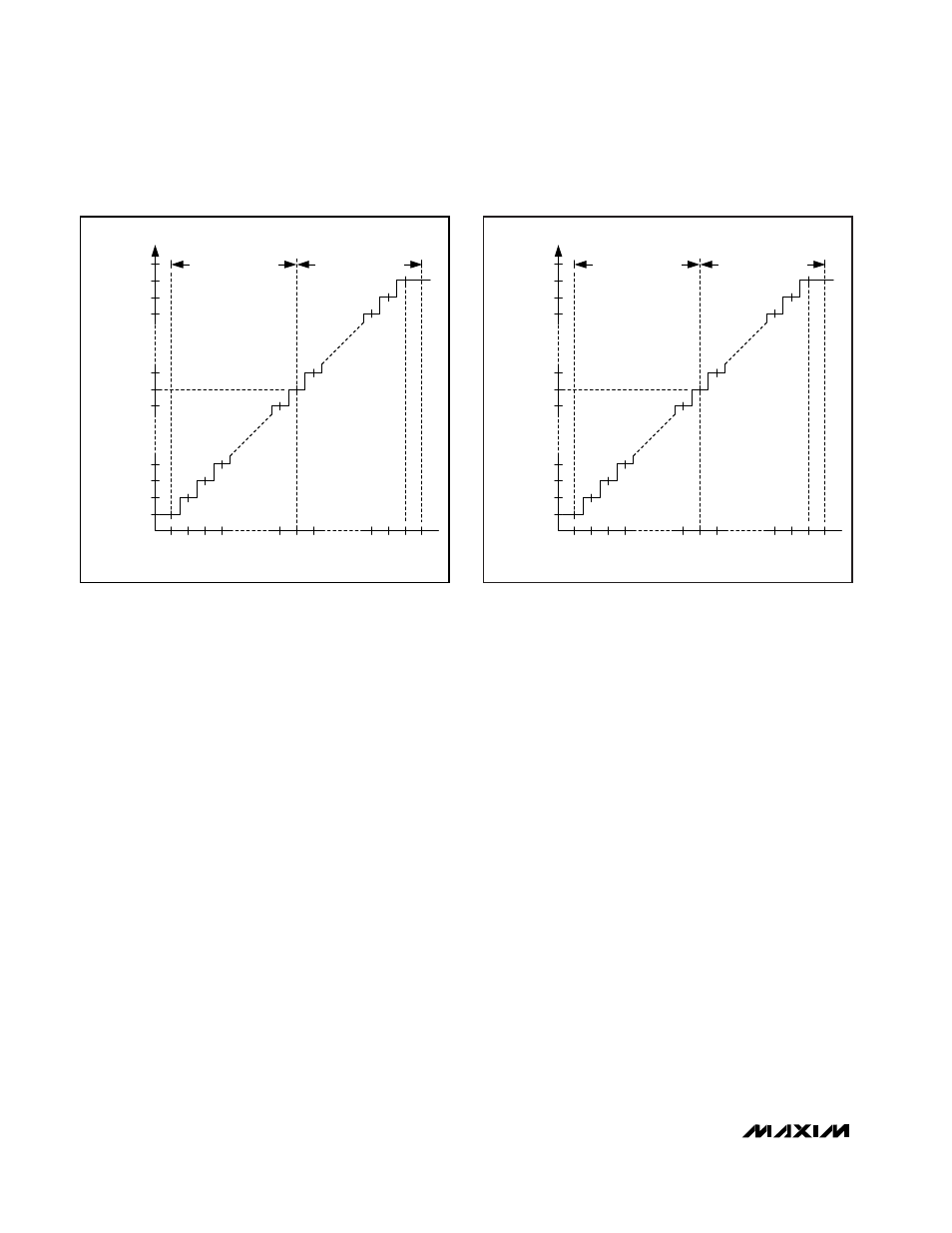
DIFFERENTIAL INPUT VOLTAGE (LSB)
TWO'S-COMPLEMENT OUTPUT CODE (LSB)
-8189
+8191
+8189
-1 0 +1
-8191
0x2000
0x2001
0x2002
0x2003
0x1FFF
0x1FFE
0x1FFD
0x3FFF
0x0000
0x0001
2/3 x (V
REFP
- V
REFN
)
2/3 x (V
REFP
- V
REFN
)
1 LSB = 4/3 x (V
REFP
- V
REFN
) / 16,384
Figure 6. Two’s-Complement Transfer Function (G/
T
= 0)
DIFFERENTIAL INPUT VOLTAGE (LSB)
GRA
Y OUTPUT CODE (LSB)
-8189
+8191
+8189
-1 0 +1
-8191
0x0000
0x0001
0x0003
0x0002
0x2000
0x2001
0x2003
0x1000
0x3000
0x3001
2/3 x (V
REFP
- V
REFN
)
2/3 x (V
REFP
- V
REFN
)
1 LSB = 4/3 x (V
REFP
- V
REFN
) / 16,384
Figure 7. Gray-Code Transfer Function (G/
T
= 1)