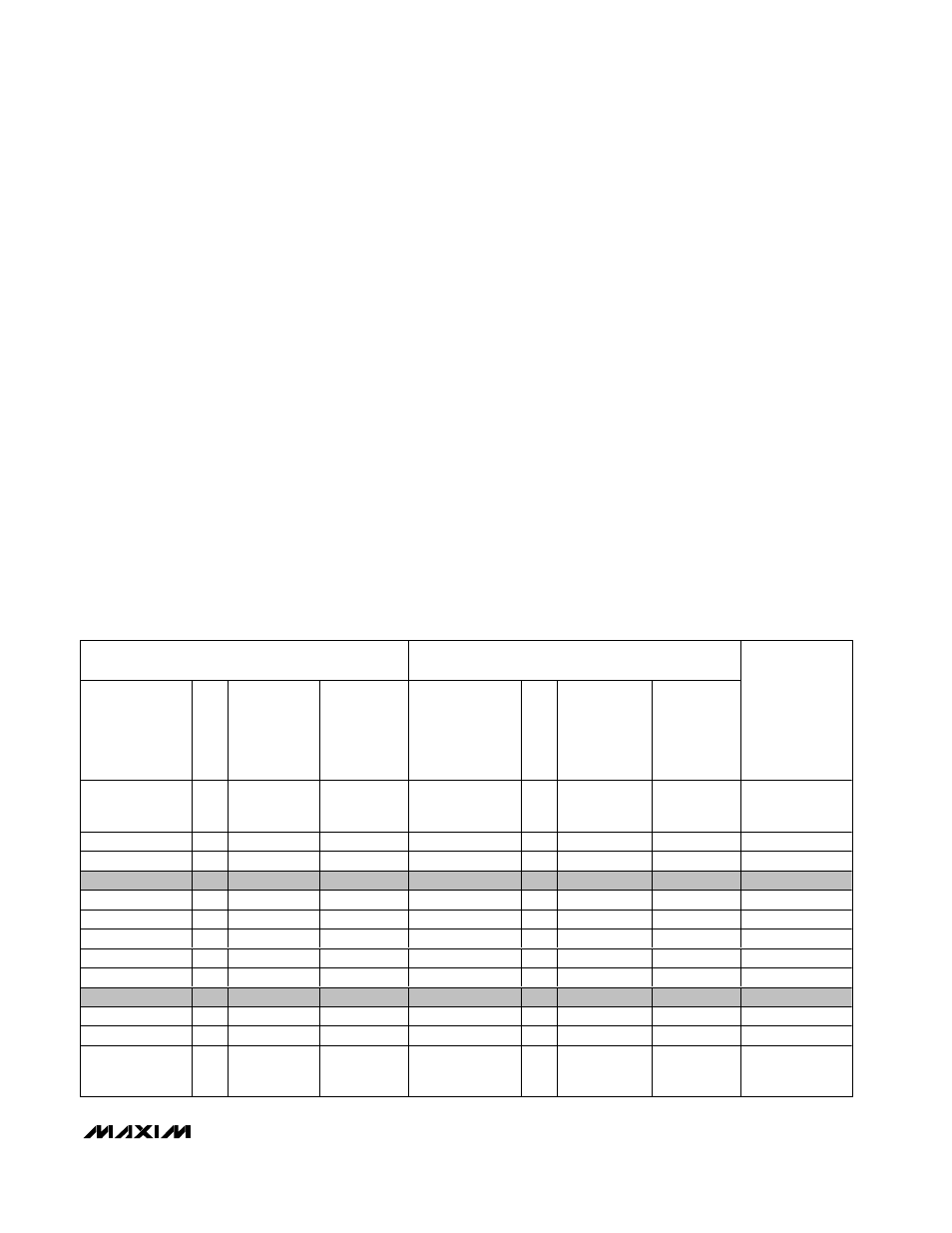
Table 3. output codes vs. input voltage – Maxim Integrated MAX12557 User Manual
Page 19
externally isolates it from heavy capacitive loads. Refer
to the MAX12557 EV kit schematic for recommendations
of how to drive the DAV signal through an external buffer.
Data Out-of-Range Indicator
The DORA and DORB digital outputs indicate when the
analog input voltage is out of range. When DOR_ is high,
the analog input is out of range. When DOR_ is low, the
analog input is within range. The valid differential input
range is from (V
REF_P
- V
REF_N
) x 2/3 to (V
REF_N
-
V
REF_P
) x 2/3. Signals outside of this valid differential
range cause DOR_ to assert high as shown in Table 1.
DOR is synchronized with DAV and transitions along
with the output data D13–D0. There is an 8 clock-cycle
latency in the DOR function as is with the output data
(Figure 5). DOR_ is high impedance when the
MAX12557 is in power-down (PD = high). DOR_ enters
a high-impedance state within 10ns after the rising edge
of PD and becomes active 10ns after PD’s falling edge.
Digital Output Data and Output Format Selection
The MAX12557 provides two 14-bit, parallel, tri-state
output buses. D0A/B–D13A/B and DORA/B update on
the falling edge of DAV and are valid on the rising edge
of DAV.
The MAX12557 output data format is either Gray code
or two’s complement depending on the logic input G/T.
With G/T high, the output data format is Gray code.
With G/T low, the output data format is set to two’s com-
plement. See Figure 8 for a binary-to-Gray and Gray-to-
binary code conversion example.
The following equations, Table 3, Figure 6, and Figure 7
define the relationship between the digital output and
the analog input.
Gray Code (G/T = 1):
V
IN_P
- V
IN_N
= 2/3 x (V
REF_P
- V
REF_N
) x 2 x
(CODE
10
- 8192) / 16,384
Two’s Complement (G/T = 0):
V
IN_P
- V
IN_N
= 2/3 x (V
REF_P
- V
REF_N
) x 2 x
CODE
10
/ 16,384
where CODE
10
is the decimal equivalent of the digital
output code as shown in Table 3.
MAX12557
Dual, 65Msps, 14-Bit, IF/Baseband ADC
______________________________________________________________________________________
19
GRAY-CODE OUTPUT CODE
(G/T = 1)
TWO’S-COMPLEMENT OUTPUT CODE
(G/T = 0)
BINARY
D13A–D0A
D13B–D0B
DOR
H EXA D ECIM A L
EQUIVALENT
OF
D13A–D0A
D13B–D0B
DECIMAL
EQUIVALENT
OF
D13A–D0A
D13B–D0B
(CODE
10
)
BINARY
D13A–D0A
D13B–D0B
DOR
HEXADECIMAL
EQUIVALENT
OF
D13A–D0A
D13B–D0B
DECIMAL
EQUIVALENT
OF
D13A–D0A
D13B–D0B
(CODE
10
)
V
IN_P
- V
IN_N
V
REF_P
= 2.418V
V
REF_N
= 0.882V
10 0000 0000 0000
1
0x2000
+16,383
01 1111 1111 1111
1
0x1FFF
+8191
>+1.023875V
(DATA OUT OF
RANGE)
10 0000 0000 0000
0
0x2000
+16,383
01 1111 1111 1111
0
0x1FFF
+8191
+1.023875V
10 0000 0000 0001
0
0x2001
+16,382
01 1111 1111 1110
0
0x1FFE
+8190
+1.023750V
11 0000 0000 0011
0
0x3003
+8194
00 0000 0000 0010
0
0x0002
+2
+0.000250V
11 0000 0000 0001
0
0x3001
+8193
00 0000 0000 0001
0
0x0001
+1
+0.000125V
11 0000 0000 0000
0
0x3000
+8192
00 0000 0000 0000
0
0x0000
0
+0.000000V
01 0000 0000 0000
0
0x1000
+8191
11 1111 1111 1111
0
0x3FFF
-1
-0.000125V
01 0000 0000 0001
0
0x1001
+8190
11 1111 1111 1110
0
0x3FFE
-2
-0.000250V
00 0000 0000 0001
0
0x0001
+1
10 0000 0000 0001
0
0x2001
-8191
-1.023875V
00 0000 0000 0000
0
0x0000
0
10 0000 0000 0000
0
0x2000
-8192
-1.024000V
00 0000 0000 0000
1
0x0000
0
10 0000 0000 0000
1
0x2000
-8192
<-1.024000V
(DATA OUT OF
RANGE)
Table 3. Output Codes vs. Input Voltage