0 block diagram, 0 gateway board physical layout, Freescale semiconductor, inc – Motorola VL-RISC MCF5202 User Manual
Page 15

MOTOROLA
GATEWAY BOARD
15
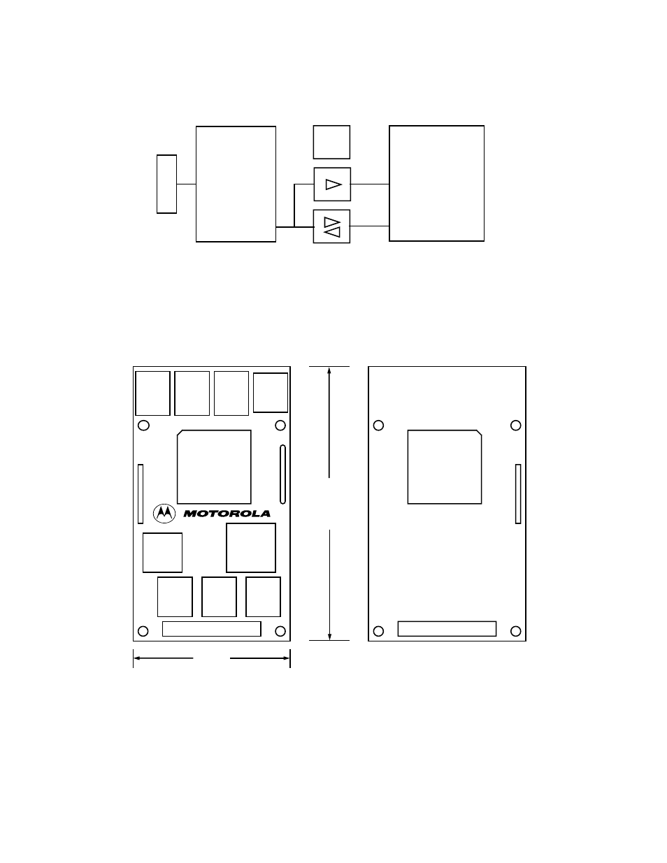
9.0 Block Diagram
Figure 5: Gateway Board Block Diagram
10.0 Gateway Board Physical Layout
Figure 6: Physical Layout (Actual Size
)
PLD
68EC000
Connector
(68-pin PLCC)
ColdFire
MCF5202
B
D
M
A
D
A/D
U1
U2
J3
U9
U6
U8
U7
U4
U5
U3
J2
ISP
ColdFire Gate
w
ay Board
S/N
1
9
10
26
44
60
61
1
26
25
2
BDM
Component Side
Solder Side
10
9
1
26
27
44
60
61
J1
43
3.5 in.
2 in.
J1
J2
J3
F
re
e
sc
a
le
S
e
m
ic
o
n
d
u
c
to
r,
I
Freescale Semiconductor, Inc.
For More Information On This Product,
Go to: www.freescale.com
n
c
.
..
