B.1 interface (fc-sca) connector signal allocation – FUJITSU MAG3091FC User Manual
Page 87
C141-E078-02EN
B - 2
B.1
Interface (FC-SCA) Connector Signal Allocation
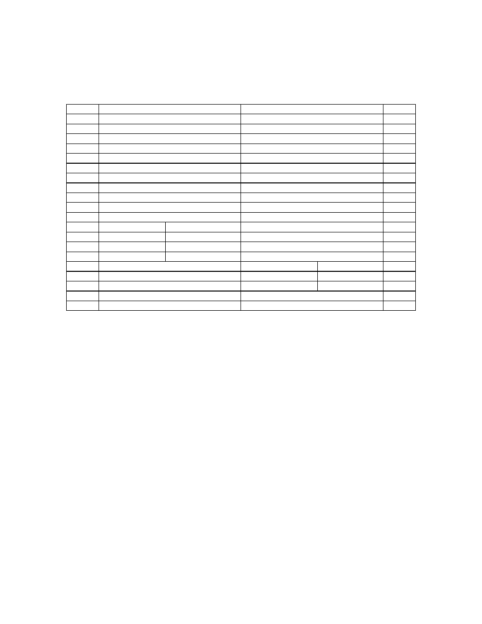
Table B.1
FC-SCA connector: CN1
Pin No.
Signal
Signal
Pin No.
01
–EN bypass port A
+12V charge
21
02
+12V
GND
22
03
+12V
GND
23
04
+12V
+PortA_in
24
05
–Parallel ESI
–PortA_in
25
06
–Drive present
GND
26
07
Active LED out
+PortB_in
27
08
–Spindle sync
–PortB_in
28
09
Start_1/Mated
GND
29
10
Start_2/Mated
+PortA_out
30
11
–EN bypass port B
–PortA_out
31
12*
SEL-6
–DSK_WR
GND
32
13*
SEL-5
–DSK_RD
+PortB-out
33
14*
SEL-4
–ENCL_ACK
–PortB-out
34
15*
SEL-3
D(3)
GND
35
16
Fault LED out
SEL-2
D(2)
36*
17
N.C
SEL-1
D(1)
37*
18
N.C
SEL-0
D(0)
38*
19
+5V
N.C
39
20
+5V
+5V charge
40
Note:
*1) Signal names in the right column of the table are those in parallel ESI operation.
See also other documents in the category FUJITSU Hardware:
- XG Series P3NK-4452-01ENZD (614 pages)
- FPCAC14C (1 page)
- MCJ3230SS (161 pages)
- MBA3073NC (138 pages)
- T5140 (102 pages)
- T5140 (76 pages)
- MAM3367MC/MP (152 pages)
- MPC3045AH (185 pages)
- MB2142-02 (23 pages)
- MB15F86UL (6 pages)
- MHS2030AT (40 pages)
- MHW2100BS (296 pages)
- MHK2060AT (227 pages)
- Disk Drives MHK2060AT (227 pages)
- MCM3064SS (170 pages)
- Mainboard D1561 (45 pages)
- MHC2040AT (219 pages)
- D1961 (45 pages)
- DISK DRIVES MHM2100AT (231 pages)
- MHR2010AT (250 pages)
- MHZ2120BJ (320 pages)
- MCE3064AP (175 pages)
- LQFP-64P (16 pages)
- Solaris PCI GigabitEthernet 3.0 (115 pages)
- MAY2036RC (94 pages)
- MAB3091 (142 pages)
- MPE3XXXAT (191 pages)
- MHV2040AH (40 pages)
- MHW2040AC (278 pages)
- ETERNUSmgr P2X0-0202-01EN (64 pages)
- VSS Hardware Provider 2.1 (134 pages)
- MAG3182FC (61 pages)
- MAU3147NC/NP (130 pages)
- MAX3147RC (94 pages)
- MHV2160BT (296 pages)
- MHV2040AT (280 pages)
- MAW3300NC/NP (130 pages)
- DeskPower E623 (50 pages)
- MAG3182LC (133 pages)
- OPTICAL DISK DRIVES MDG3064UB (42 pages)
- MHF2021AT (225 pages)
- MHR2040AT (40 pages)
- Single Drive FTM7926FB (1 page)
- PG-FCS103 (98 pages)
- MAS3735FC (114 pages)