Tm1 multiple-mt90840 sub-mode (pfdi), Asynchronous parallel port with st-bus clock slave, Preliminary information – Mitel DISTRIBUTED HYPERCHANNEL MT90840 User Manual
Page 12
MT90840
Preliminary Information
2-242
TM1. This allows for flexible round-trip data delays in
star or ring type networks. An elastic buffer on the
receive parallel port compensates for the difference
in phase between PPFRi/PCKR and F0i/C4. The
elastic buffer can also tolerate up to 50
µ
sec +/- 25
µ
sec) of clock drift and jitter before the buffer
re-syncs and Rx Path data is corrupted. (Data
corruption is flagged by the FSA interrupt source.)
The Bypass Path data (PDi to PDo) also passes
through the elastic buffer in TM1.
In TM1, the MT90840's SPCKo clock output is not
used.
TM1 Multiple-MT90840 Sub-Mode (PFDI)
For TM1 applications which require more serial
channels than are provided by a single MT90840, it
is possible to operate multiple MT90840 in parallel.
To do this, one MT90840 must control the
F0i-to-PPFTo timing (normal TM1), and the
remaining MT90840s must synchronize to the first by
using PPFTi as an input reference. The device
providing the reference will have the PFDI bit in the
TIM Register set low (normal TM1). All other
MT90840s will have PFDI set high (forcing PPFT to
be an input).
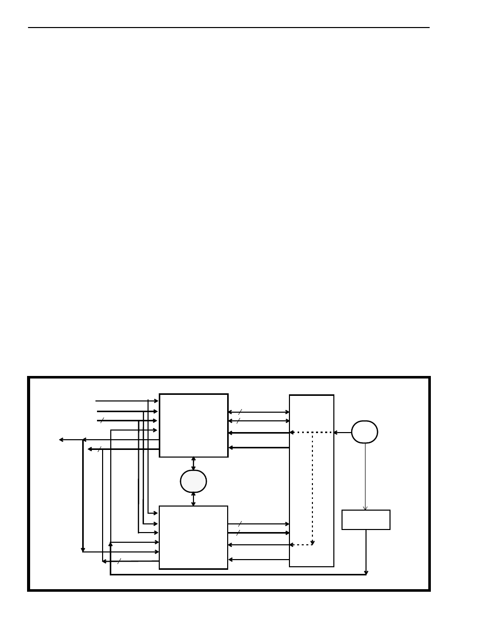
Figure 5b shows this mode using two MT90840s;
additional MT90840s (with PFDI set high) may be
added. This sub-mode allows the serial ports of the
multiple MT90840 to share one timing source, and
the synchronized parallel output ports to be
connected together on one bus.
The TM1 Multiple-MT90840 sub-mode is not
available for operation at 6.48 Mbyte/s.
Timing Mode 2 (TM2) - Ring Slave
Asynchronous Parallel Port With ST-BUS Clock
Slave
Timing Mode 2 is used where the main TDM clock
reference resides on the parallel port side of the
system. (An example is a node on a ring which is
slaved to the ring clock.) Timing on the serial port is
tightly tied (slaved) to the receive parallel port, and
the transmit parallel port is clocked by the receive
parallel port clock. In TM2, the PCKT input is not
used. See Figure 6a for a connection example.
In TM2, the MT90840 timing is controlled by the
parallel port frame pulse (PPFRi) and clock (PCKR).
The MT90840 generates the parallel port output
frame pulse (PPFTo) and the serial port output frame
pulse (F0o) locked to PPFRi. Both the transmit
parallel port and the serial port are fixed in phase
relative to the receive parallel port, and therefore no
elastic buffer is required. A fixed offset exists
between PPFRi and F0o due to parallel-to-serial
conversion, and between F0o and PPFTo due to
serial-to-parallel conversion delay. Total offset
between PPFRi and PPFRo is about 12
µ
sec (and
the Bypass Path data delay is therefore also about
12
µ
sec).
Figure 5b - TM1 Multiple-MT90840 Configuration
8
8
8 kHz RX
RX Data
TX Clock
8 kHz TX
TX Data
PCKR
PPFRi
PDi0-7
PCKT
PPFTo
PDo0-7
STi0-7
STo0-7
F0i
C4/8R1
8 STi/o 0-7
8
STi/o 0-7
4.096
MT90840
RX Clock
CPU
ST-BUS
Components
or 8.192 MHz
8 kHz
8
8 kHz TX
Data TX
PCKR
PPFRi
PDi0-7
PCKT
PPFTi
PDo0-7
STi0-7
STo0-7
F0i
C4/8R1
8 STi/o 0-7
8
STi/o 0-7
4.096
MT90840
or 8.192 MHz
8 kHz
PFDI = 0
PFDI = 1
8 kHz
Source
PLL
TX Clock
TX Clock