Chapter 2, System components, Block diagram – Lanner LEC-7110 User Manual
Page 7: Embedded and industrial computing
7
System Components
Chapter 2
Embedded and Industrial Computing
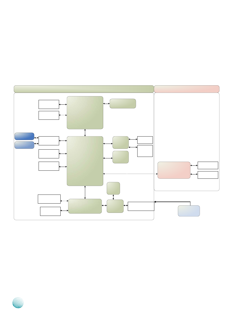
Block Diagram
The block diagram depicts the relationships among the
interfaces and modules on the motherboard..
LEB-7110
LEB-7110
LEK-HDA1
Realtek ALC886
2x 1/8 Phone Jack
DDR3 800/1067
1x SO-DIMM up to 4GB
GbE Controller
2x Intel 82583
Flash BIOS
MCU
(32-bit ARM
Cortex-M0
microcontroller)
Processor
Intel
D2550
(BGA)
PCH
NM10
Fintek
81865
2x PCIe
SPI
Flash
(Store the status of
the DIO before
system reboot)
1x 2.5" HDD/SSD
1x SATA DOM
VGA
Up to 1920x 1200
HDMI
SATA Connector
2x SATA Connectors
Mini PCIe with
SIM card Reader
1x Socket
USB 2.0
2x Port-A in front
2x Port-A in rear
2x Pin Header
Serial Port
2x pin header for RS-232
H/W Monitor
WDT
SATA
PCIe
USB
USB
LAN 1
RJ-45
LAN 2
RJ-45
(reserved pin
header for PoE
splitter)
Digital I/O
4x in, 4x out, terminal blocks
100mA for each output port
Power Adapter
+12V AC to DC Power
(DC-Jack with lock)
Audio Output
1/8 Phone Jack
Mic Input
1/8 Phone Jack
+12V