Chapter 3, Board layout, Jumper settings – Lanner LEC-7110 User Manual
Page 14: Sc1t1
14
Board Layout
Chapter 3
Embedded and Industrial Computing
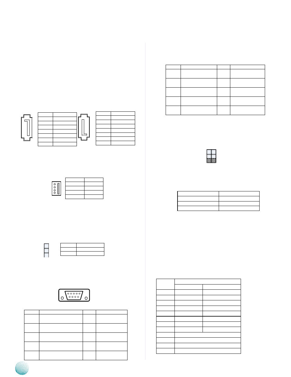
RS-232 Serial Port COM2 (JCOMB1): It is a RS-232 port
with a internal pin header.
COMA1 Pin 9 Function Selection (SC1T1): The Pin No. 9
of RS-232 can be altered to supply power. J
LAN1_1/LAN1_2: Dual RJ-45 with LED: The LAN ports
are provided by Intel 82583 Ethernet Controllers. The
following lists its main features:
The Preboot eXecution Environment (PXE) remote
•
boot support
TCP segmentation offload
•
TCP, UDP, IPv4 checksum offload
•
Supports IEEE 802.1Q VLAN tagging
•
Pin No. Description
Fast Ethernet Gigabit Ethernet
1
TX+
MD0+
2
TX-
MD0-
3
RX+
MD1+
4
T45
MD2+
5
T45
MD2-
6
RX-
MD1-
7
T78
MD3+
8
T78
MD3-
9
10-/100-/1000+
10
10+/100+/1000-
11
Link+/ACT-
12
Link-/ACT+
Jumper Settings
Serial-ATA Connector (SATA1, SATA2): It is for connecting
a 2.5’’ harddisk to be served as your system’s storage. It
can support SATA II which features Data transfer rates up to
3.0 Gb/s (300 MB/s). Note that SATA I supports SATA DOM
connection and it has a jumper to switch the powermode
of this port.
4-pin Serial-ATA Power Connector (PW1): It is for
connecting the SATA power cord (for SATA2 connector).
SATA1Power Mode Selection (JSATA1): The SATA1
interface’s pin can be switched by this jumper to supply
power to a SATA DOM.
RS-232 Serial Port COM1 (JCOMA1): It is a RS-232 port
through the D-SUB9 connector.
Pin No.
Pin Name
Pin No.
Pin Name
1
Data Carrier Detect
(DCDA# )
6
Data Set Ready
(DSRA # )
2
Receive Data
( RXDA )
7
Request To Send
(RTSA # )
3
Transmit Data
(TXDA)
8
Clear To Send
(CTSA # )
4
Data Terminal Ready
(DTRA #)
9
Ring Indicator
(RIA # )
5
Ground
(GND )
RS-232 Pin 9 Function
JP1, JP2
+5V
1-2
+12V
3-4
RI#(Default)
5-6
LEB-7110
Pin No.
Function
1
+12V
2
GND
3
GND
4
+5V
SC1T1
1
3
5
2
4
6
Pin No.
Function
1-2
GND (Default)
2-3
+5V
1 2 3 4 5
6 7 8 9
Pin No.
Function
1
GND
2
TX+
3
TX-
4
GND
5
RX-
6
RX+
7
SATA Power
7
6
5
4
3
2
1
SATA1
1
2
3
4
5
6
7
SATA2
Pin No.
Function
1
GND
2
TX+
3
TX-
4
GND
5
RX-
6
RX+
7
SATA Power
4
3
2
1
3
2
1
Pin No.
Pin Name
Pin No.
Pin Name
1
Data Carrier Detect
(DCDB #)
6
Clear To Send
(CTSB #)
2
Data Set Ready
(DSRB #)
7
Data Terminal Ready
(DTRB #)
3
Receive Data
(RXDB)
8
Ring Indicator
(RIB #)
4
Request To Send
(RTSB #)
9
Ground
5
Transmit Data
(TXDB)
10
KEY