Chapter 3, Board layout – Lanner LEC-7110 User Manual
Page 15
15
Board Layout
Chapter 3
Embedded and Industrial Computing
Dual USB Type A Connector (USB1/USB3):
USB 2.0 Pin Header (USB2):
MCU Communication Setting (SC3T1): MCU
communication setting jumper
MCU Debug Port (JTAG1): The MCU is provided by NXP’s
LPC1110 which is a ARM-Cortex-M0 based, low-cost 32-bit
microcontroller for 8/16-bit applications. It has a 4 KB on-
chip flash programming memory. The MCU and its flash
will help to retain the DIO last state even when the system
reboots or shuts down.
Clear CMOS jumper (JCCMOS1): It is for clearing the
CMOS memory.
Digital I/O (DI1)
Digital IN/OUT(DIO1) Connector: The 8 pins of digital
Input/Output (GPIO) support input and output operations
through the 2x5-pin terminal block.
TTL Level is +5V; Maximum input/output current for
each port is 100mA
Input/Output Voltage
Logic
Register
Digital_IN:
0~0.7V
Digital_Out:
0V
Low
0
Digital_IN:
2~5V
Digital_Out:
5V
High
1
The default BIOS value is 0 for digital_IN and 1for Digi-
tal_Out
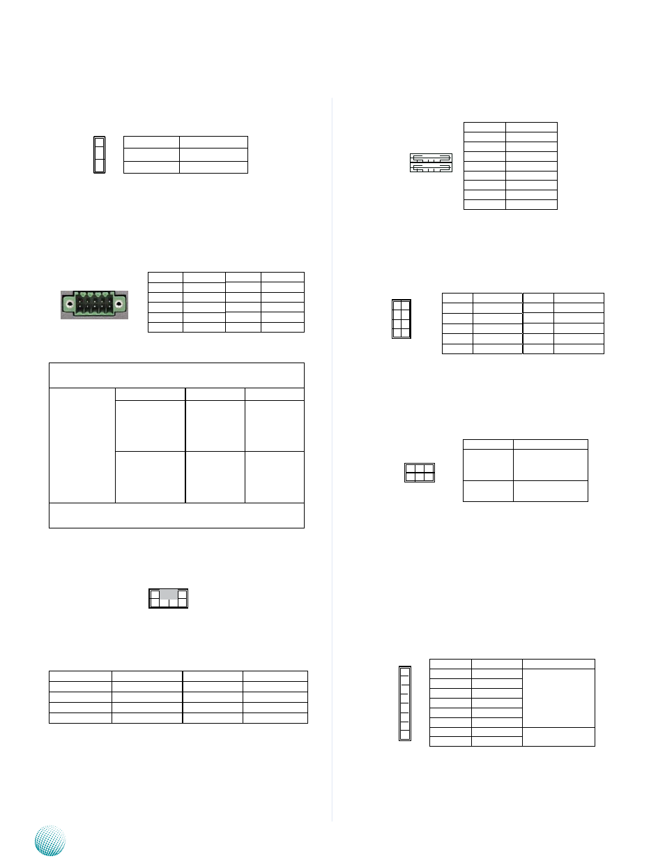
PS/2 Keyboard and Mouse (KB1)
Pin No.
Description
Pin No.
Description
1
VCC
2
MSCLK
3
MSDATA
4
KEY
5
KBDATA
6
KEY
7
GND
8
KBCLK
Pin No. Pin Name
1
Input0
3
Input1
5
Input2
7
Input3
9
GND
Pin No. Pin Name
2
Output0
4
Output1
6
Output2
8
Output3
10
GND
Pin No.
Pin Name
1-2
Normal (Default)
2-3
Clear CMOS
1
2
3
Pin No.
Pin Name
1
USB_VCC1
2
-USB
3
+USB
4
GND
5
USB_VCC2
6
-USB
7
+USB
8
GND
1 2 3 4
5 6 7 8
Pin No. Pin Name
1
USB_VCC
3
KEY
5
-USB
7
+USB
9
GND
Pin No. Pin Name
2
GND
4
+USB
6
-USB
8
KEY
10
USB_VCC
9
7
5
3
1
10
8
6
4
2
PIN NO.
DESCRIPTION
1-3 2-4
Internal
RS232(COM3)
(default)
3-5 4-6
From JTAG1 RS232
(debug only)
2 4 6
1 3 5
1
2
3
4
5
6
7
8
Pin No.
Pin Name
Debug Tools
1
ICE_DATA
FOR ICE Debug
2
ICE_CLK
3
ICE_RST#
4
GND
5
MCU_PRO
6
MCU_VCC
7
ICE_RX
For Ext RS232
8
ICE_TX
1 3 5 7
2 4 6 8
1 3 5 7 9
2 4 6 8 10