Functional description, Inputs and outputs, Microcontroller – Grass Valley 2000GEN User Manual
Page 19
2000GEN Instruction Manual
19
Functional Description
Functional Description
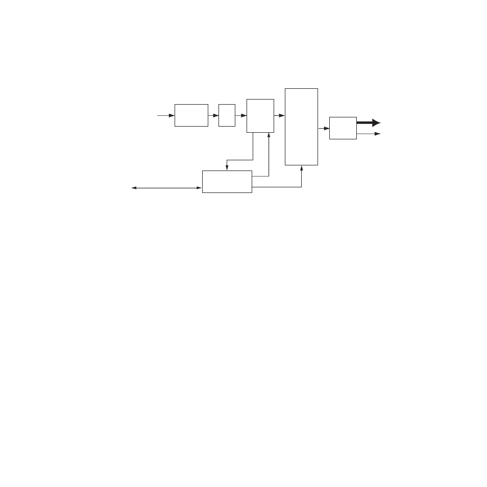
A block diagram of the 2000GEN is shown in
.
Figure 12. 2000GEN Block Diagram
Inputs and Outputs
The module input accepts a PAL-B or NTSC black-burst signal from the
Reference In BNC on the rear of the Kameleon frame. The reference signal
is first processed in a clamp and gain circuit. It is then digitized and locked
in a Burst Genlock circuit before entering output logic processing. Output
phase adjustments of up to one color frame can be made to the timing
signal through the remote monitoring GUI.
The module outputs a low-jitter 27 MHz reference clock which is distrib-
uted through differential LVDS (low voltage differential signal) lines to
each front module slot. It also generates a common reference pulse timing
stream containing a reference field pulse, frame bit, color-frame bit and
AES 5 sequence bits for distribution throughout the frame.
Microcontroller
The primary purpose of the microcontroller section is to provide remote
control and monitoring capability for the 2000GEN.
8172_04
Gain and
Clamp
A
to
D
Burst
Genlock
Output
Logic
Output
Drivers
Microcontroller
12 x LVDS Clock
Delay, Output Signal path selection
Input Signal path selection
Signal present, locked, signals
Black Burst
Input
Remote control/monitoring
Locking mode
Bus
Timing