Smt700 block diagram, 4 functional description, 1 block diagram – Sundance SMT784 User Manual
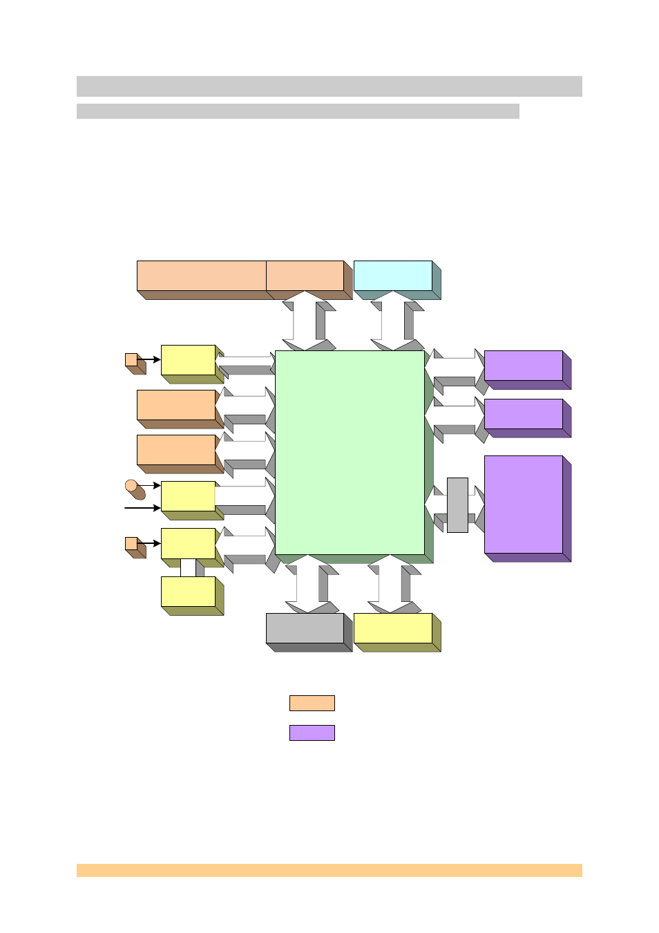
Page 9: Figure 1: smt700 block diagram
User Manual SMT784
Last Edited: 19/03/2009 14:12:00
4 Functional Description
4.1 Block Diagram
The major elements of the SMT784 can be broken down into the two main modules
it is comprised of: the SMT700 and SMT384. The SMT700 PXIe carrier board block
diagram can be viewed below.
Custom Front Panel
Ethernet
PHY
SFF Connectors
2 lanes of Fibre
2 x 2.5Gb/s
serial links
Config
CPLD
& USB
Clock
generation
1.5GHz SATA
2.5GHz RSL
SATA Connectors
2 lanes of RSL
DDR2
1GByte 220MHz
SLB
120 I
/O
pi
ns
FPGA
Virtex5 LXT-50
FF1136 package
PXIe Connector
8 lanes of 2.5Gb/s
8 x 2.5Gb/s
serial links
6
4
bi
t dat
a
1
9
ad
dr
ess
13 c
ont
rol
PXI Control
(Trigger, Clk, etc)
32 bit PCI
33/66MHz
(option)
2 x 2.5Gb/s
serial links
Ext clk
USB
PXIe ref
512Mbit
flash
RSL Connector
4 lanes of 2.5Gb/s
4 x
2.
5Gb/s
s
e
ri
al
l
inks
LEDs and
Misc. I/O
SHB
(opt
ion)
Front Panel
Connector
Rear Card
Connector
SMT700 Block Diagram
Ethernet
Figure 1: SMT700 Block Diagram
- SMT107 (16 pages)
- SMT6035 v.2.2 (39 pages)
- SMT6012 v.4.6 (22 pages)
- FC100 (12 pages)
- FC108 v.1.1 (10 pages)
- SMT6065 v.4.0 (45 pages)
- FFT v.2.1 (19 pages)
- SMT111 (18 pages)
- SMT118LT (10 pages)
- SMT118 (20 pages)
- SMT123-SHB (13 pages)
- SMT128 (15 pages)
- SMT145 (18 pages)
- SMT148 (35 pages)
- SMT130 v.1.0 (46 pages)
- SMT148FX (48 pages)
- SMT310Q (55 pages)
- PARS (70 pages)
- SMT166-FMC (52 pages)
- SMT166 (44 pages)
- SMT300Q v.1.6 (61 pages)
- SMT310 v.1.6 (50 pages)
- SMT317 (24 pages)
- SMT326v2 (24 pages)
- SMT338 (19 pages)
- SMT349 (32 pages)
- SMT339 v.1.3 (27 pages)
- SMT338-VP (22 pages)
- SMT358 (25 pages)
- SMT351T (37 pages)
- SMT351 (25 pages)
- SMT350 (45 pages)
- SMT362 (30 pages)
- SMT365G (23 pages)
- SMT364 (37 pages)
- SMT373 (15 pages)
- SMT368 (24 pages)
- SMT370v3 (46 pages)
- SMT377 (22 pages)
- SMT381 2007 (31 pages)
- SMT381-VP (81 pages)
- SMT387 (42 pages)
- SMT391 (18 pages)
- SMT384 (47 pages)
- SMT390-VP (55 pages)