Sundance SMT784 User Manual
Page 17
User Manual SMT784
Page 17 of 31
Last Edited: 19/03/2009 14:12:00
5.14 Switch 1 Flash Settings
The following table represents the various switch settings for switch 1:
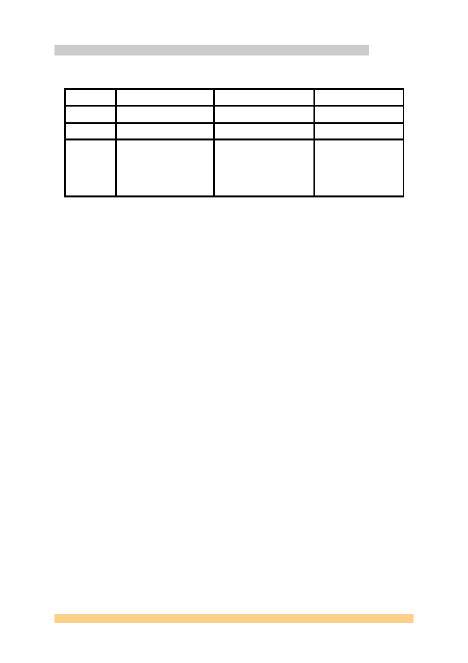
Table 3 Common Configurations of Switch 1
Switch 1 (SW1) on the front side of the SMT784 controls flash read and write access
for the carrier board, as well as selecting which flash address to boot from. POS 1
sends a hard reset to the CPLD instructing it to reconfigure the FPGA according to
which address in flash is selected. The combined positions of POS 4 and POS 3 tell
the CPLD how the FPGA is to be configured at power up according to Table 3.
After power up, a new bit-stream can be sent via USB by using Diamond Server, or
by first uploading the new firmware to flash with the SMT6002, then performing a
reset with POS 1.
POS 2 selects which address in flash the CPLD is going to configure the FPGA from.
The flash address contents can be viewed and written to by using the SMT6002. POS
2 ON boots from the backup SMT700 firmware (flash address 0x0), while off selects
the SMT784 firmware (flash address 0x800000).
The SMT700 default firmware is provided as a backup bit-stream in the event that
user-modified firmware at address 0x800000 in flash does not work as expected.
Sundance therefore suggests that when writing custom firmware to flash, do not
write to address 0x0 - only write to address 0x800000.
POS 4
ON OFF
OFF
POS 3
ON OFF ON
POS 1
Reset Reset Reset
Flash
condition
PCB configured to
boot from flash and
allow for serial
RD/WR through PCI
(SMT6002)
FPGA can be
configured via a bit-
stream uploaded on
the USB link
(Diamond Server)
Flash access is
available for
RD/WR only via
the USB link using
the SMT6002