Sundance SMT784 User Manual
Page 18
User Manual SMT784
Page 18 of 31
Last Edited: 19/03/2009 14:12:00
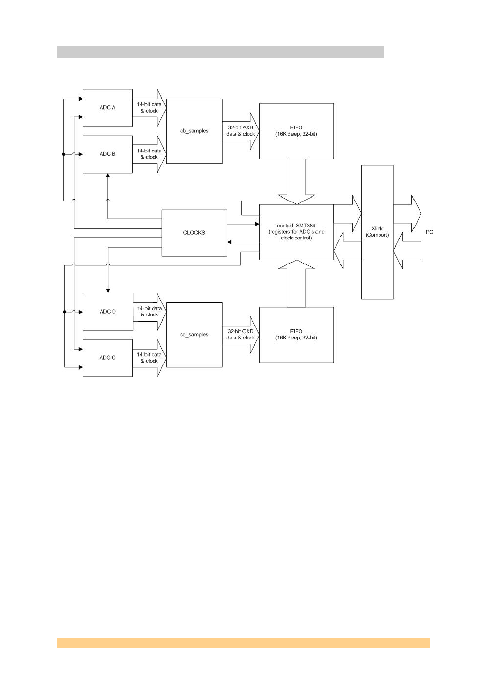
5.15 ADC Data Flow
The flow of ADC data in the SMT784:
Figure 5 ADC Data Flow
The Control Registers contained in the FPGA (control_SMT384) control the complete
functionality of the SMT384. Registers are written to/from the PC via the X-Link
interface. Contents of the registers or samples from the ADC’s can be read back
from the FPGA by choosing which output is desired. By changing the default
firmware, samples from the ADC’s can optionally be routed to the RSL links, SHB,
SATA, etc.
Details of the registers functions, word format and a memory-map of the FPGA can
be found in the
SMT384 User Guide
.
Serial control signals are routed from the registers to the ADC’s and to the clock
distribution system for desired configuration. Samples and the clock output from
the ADC’s are then combined onto two different 32-bit buses, one containing
samples from channels A and B, the other bus containing samples from channels C
and D. In order to prevent loss of data, a 16K buffer is implemented to feed the
samples to the control_SMT384 block. When control registers are programmed to be
returned to the PC (selected by Host application), the ADC FIFO’s are held in reset.
Upon selection of the desired channel output, the buffer resumes operation.