4 functional description, 1 block diagram, 2 module description – Sundance SMT399-160 User Manual
Page 9: Functional description, Block diagram, Module description, Figure 2 - smt399-160 block diagram
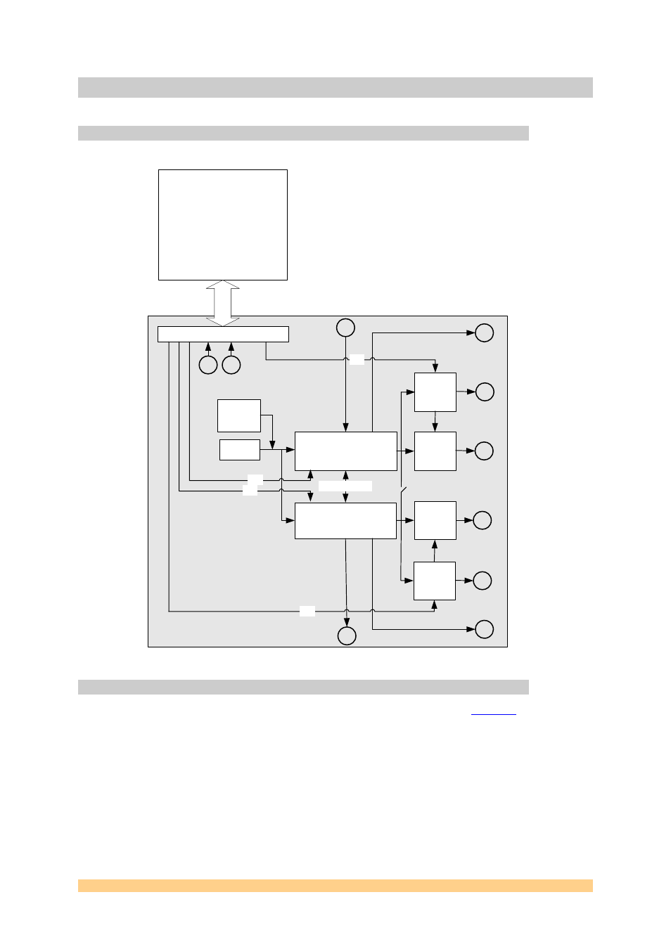
4 Functional Description
In this part, we will see the general block diagram and some comments on the main entities.
4.1 Block Diagram
The following diagram shows the block diagram of the SMT399-160.
Sundance SLB base
module (SMT338-VP,
SMT398-VP or SMT368
for example)
68
I
/O
pi
ns
+3.3
V
, +5V
SMT399-160 SLB
A0
1xAD9954 DDS (Channel A)
14-bit @ 400MSPS
48-pin TQFP
On-board
Crystal
AD8370
VGA
I/Os
B0
1xAD9954 DDS (Channel B)
14-bit @ 400MSPS
48-pin TQFP
I/Os
Synchronisation
I/Os
I/Os
Syn
in
Syn
out
Daughter Module - SMT399-160
AD8370
VGA
A1
AD8370
VGA
AD8370
VGA
B1
External
Reference
(Option)
Trig
A
Trig
B
squ
are
A
squ
are
B
Figure 2 - SMT399-160 Block Diagram.
4.2 Module Description
The module is built around two Direct Digital Synthesizers (DDS): two
.
The AD9954 is a DDS featuring 14-bit DAC operating at up to 400MSPS. It forms a digitally
programmable high frequency synthesizer capable of generating an analog output sinusoidal
waveform at up to 160MHz. The AD9954 provides fast frequency hopping and fine-tuning
resolution (32-bit frequency tuning word). The AD9954 includes an integrated 1024x32 static
RAM to support flexible frequency sweep capability in several modes. It also supports a user
defined linear sweep mode of operation. The frequency resolution of the AD9954 is 0.0931
Hz when clocked at 400MHz. Both analog outputs can be linked together via jumpers in
order to generate a dual tone signal.
User Manual SMT399-160
Last Edited: 24/05/2007 17:12:00