7 dds0 register – 0x6 – control function register, Dds0 register – 0x6 – control function register – Sundance SMT399-160 User Manual
Page 20
0
Gain Mode
Gain
Default
‘0’ ‘0000000’
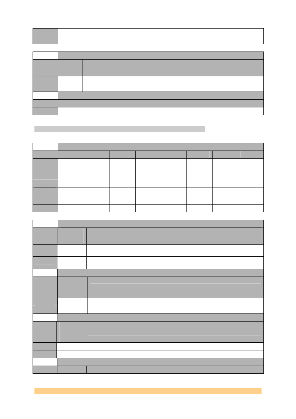
VGA3 Register – 0x5
Setting
Gain
Mode
(Bit 7)
Description
0
0
LG Mode: Low Gain. The Gain can be from -11 to +17dBs.
1
1
HG Mode: Low Gain. The Gain can be from +6 to +34dBs.
VGA3 Register – 0x5
Setting
Bits 6-0
Description
0
Gain value (Binary). The scale is from -11 to +17dBs (LG Mode) or from +6 to +34dBs (HG Mode).
5.4.7 DDS0 Register – 0x6 – Control Function Register.
For more details, refer to AD9954 datasheet.
DDS0 Register – 0x6 – Control Function Register
Byte
Bit 7
Bit 6
Bit 5
Bit 4
Bit 3
Bit 2
Bit 1
Bit 0
0
Digital
Power
Down
Comp
Power
Down
DAC
Power-
Down
Clock
Input
Power-
down
External
Power-
down
Mode
Linear
Sweep No
Dwell
SYNC_CLk
Out
Disable
Not Used
Default
‘0’ ‘0’ ‘0’ ‘0’ ‘0’ ‘0’ ‘0’ ‘0’
1
Load SRR
@ IO UD
AutoClear
Freq
Accum
AutoClear
Phase
Accum
Enable
Sine
Output
Clear Freq
Accum
Clear
Phase
Accum
SDIO
Input Only
LSB First
Default
‘0’ ‘0’ ‘0’ ‘0’ ‘0’ ‘0’ ‘0’ ‘0’
DDS0 Register – 0x6 – Control Function Register
Setting
Load SRR
@IO UD
(Bit 15)
Description
0
0
The Linear Sweep Ramp Rate timer is loaded only upon timeout and is not loaded due to an Io
Update input signal.
1
1
The Linear Sweep Ramp Rate timer is loaded only upon timeout and is loaded due to an Io
Update input signal.
DDS0 Register – 0x6 – Control Function Register
Setting
Auto Clear
Freq
Accum
(Bit 14)
Description
0
0
The state of the frequency accumulator remains unchanged.
1
1
Clears the frequency accumulator for one cycle on an IO Update signal.
DDS0 Register – 0x6 – Control Function Register
Setting
Auto Clear
Phase
Accum
(Bit 13)
Description
0
0
The state of the phase accumulator remains unchanged.
1
1
Clears the phase accumulator for one cycle on an IO Update signal.
DDS0 Register – 0x6 – Control Function Register
Setting
Enable
Description
User Manual SMT399-160
Page 20 of 39
Last Edited: 24/05/2007 17:12:00