2 reading and writing registers, 3 memory map, Reading and writing registers – Sundance SMT399-160 User Manual
Page 14: Memory map, Figure 8 – control register read sequence
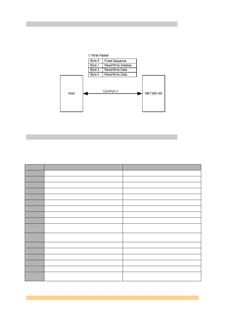
5.2 Reading and Writing Registers
Control packets are sent to the SMT399-160 over Comport3 only in the standard firmware.
This is a bi-directional interface. The format of a ‘Read Packet’ is the same as that of a write
packet.
Figure 8 – Control Register Read Sequence.
5.3 Memory Map
The write packets must contain the address where the data must be written to and the read
packets must contain the address where the required data must be read. The following figure
shows the memory map for the writable and readable Control Registers on the SMT399-160:
Address
Writable Registers
Readable Registers
0x00
Reset and Update Register.
Reserved.
0x01
DDS0 and 1 Profile Register.
DDS0 and DDS1 Profile Register.
0x02
VGA0.
Read-back (FPGA Register) VGA0.
0x03
VGA1.
Read-back (FPGA Register) VGA1.
0x04
VGA2.
Read-back (FPGA Register) VGA2.
0x05
VGA3.
Read-back (FPGA Register) VGA3.
0x06
DDS0 – Register 0 (0x0) – Control Function Register.
Read-back (FPGA Register) DDS0 – Register 0 (0x0).
0x07
DDS0 – Register 1 (0x1) – Control Function Register.
Read-back (FPGA Register) DDS0 – Register 1 (0x1).
0x08
DDS0 – Register 2 (0x2) – Control Function Register.
Read-back (FPGA Register) DDS0 – Register 2 (0x2).
0x09
DDS0 – Register 3 (0x3) – Amplitude Scale Factor
Register.
Read-back (FPGA Register) DDS0 – Register 3 (0x3).
0x0A
DDS0 – Register 4 (0x4) – Amplitude Ramp Rate
Register.
Read-back (FPGA Register) DDS0 – Register 4 (0x4).
0x0B
DDS0 – Register 5 (0x5) – Frequency Tuning Word 0.
Read-back (FPGA Register) DDS0 – Register 5 (0x5).
0x0C
DDS0 – Register 6 (0x6) – Frequency Tuning Word 0.
Read-back (FPGA Register) DDS0 – Register 6 (0x6).
0x0D
DDS0 – Register 7 (0x7) – Phase Offset Word.
Read-back (FPGA Register) DDS0 – Register 7 (0x7).
0x0E
DDS0 – Register 8 (0x8) – Frequency Tuning Word 1.
Read-back (FPGA Register) DDS0 – Register 8 (0x8).
0x0F
DDS0 – Register 9 (0x9) – Frequency Tuning Word 1.
Read-back (FPGA Register) DDS0 – Register 9 (0x9).
0x10
DDS0 – Register A (0xA) – RAM Segment Control
Word 0.
Read-back (FPGA Register) DDS0 – Register A (0xA).
User Manual SMT399-160
Page 14 of 39
Last Edited: 24/05/2007 17:12:00