8 dds0 register – 0x7 – control function register, Dds0 register – 0x7 – control function register – Sundance SMT399-160 User Manual
Page 22
4)
0
0
The clock input circuitry is enabled.
1
1
The Clock input circuitry is disabled.
DDS0 Register – 0x6 – Control Function Register
Setting
External
Power
Down (Bit
3)
Description
0
0
Only digital logic and DAC are powered down when PWRDWNCTL pin is high.
1
1
All functions are powered down when PWRDWNCTL pin is high.
DDS0 Register – 0x6 – Control Function Register
Setting
Linear
Sweep
(Bit 2)
Description
0
0
The linear sweep no dwell function is inactive.
1
1
The linear sweep no dwell function is active.
DDS0 Register – 0x6 – Control Function Register
Setting
SYNC_CLK
out disable
(Bit 1)
Description
0
0
The SYNC_CLK pin is active.
1
1
The SYNC_CLK pin assumes a static 0.
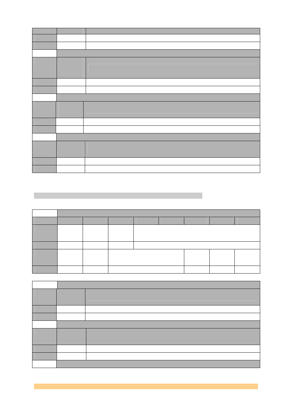
5.4.8 DDS0 Register – 0x7 – Control Function Register.
For more details, refer to AD9954 datasheet.
DDS0 Register – 0x7 – Control Function Register
Byte
Bit 7
Bit 6
Bit 5
Bit 4
Bit 3
Bit 2
Bit 1
Bit 0
0
Autoatic
Sync
Enable
Software
Manual
Sync
Linear
Sweep
Enable
Not Used
Default
‘0’ ‘0’ ‘0’
‘00000’
1
RAM
Enable
RAM Dest
is Phase
Word
Internal Profile Control
Load ARR
OSK
Enable
Auto OSK
Keying
Default
‘0’ ‘0’
‘000’
‘0’ ‘0’ ‘0’
DDS0 Register – 0x7 – Control Function Register
Setting
RAM
Enable
(Bit 15)
Description
0
0 The
RAM
disabled.
1
1
The RAM is active for operation.
DDS0 Register – 0x7 – Control Function Register
Setting
RAM
Destination
(Bit 14)
Description
0
0
The RAM drives the phase accumulator.
1
1
The RAM drives the phase-offset adder.
DDS0 Register – 0x7 – Control Function Register
User Manual SMT399-160
Page 22 of 39
Last Edited: 24/05/2007 17:12:00