Block diagram, Figure 1 - block diagram, Xilinx fpga virtex-ii – Sundance SMT377 User Manual
Page 8
Version 1.1
Page 8 of 22
SMT377 User Manual
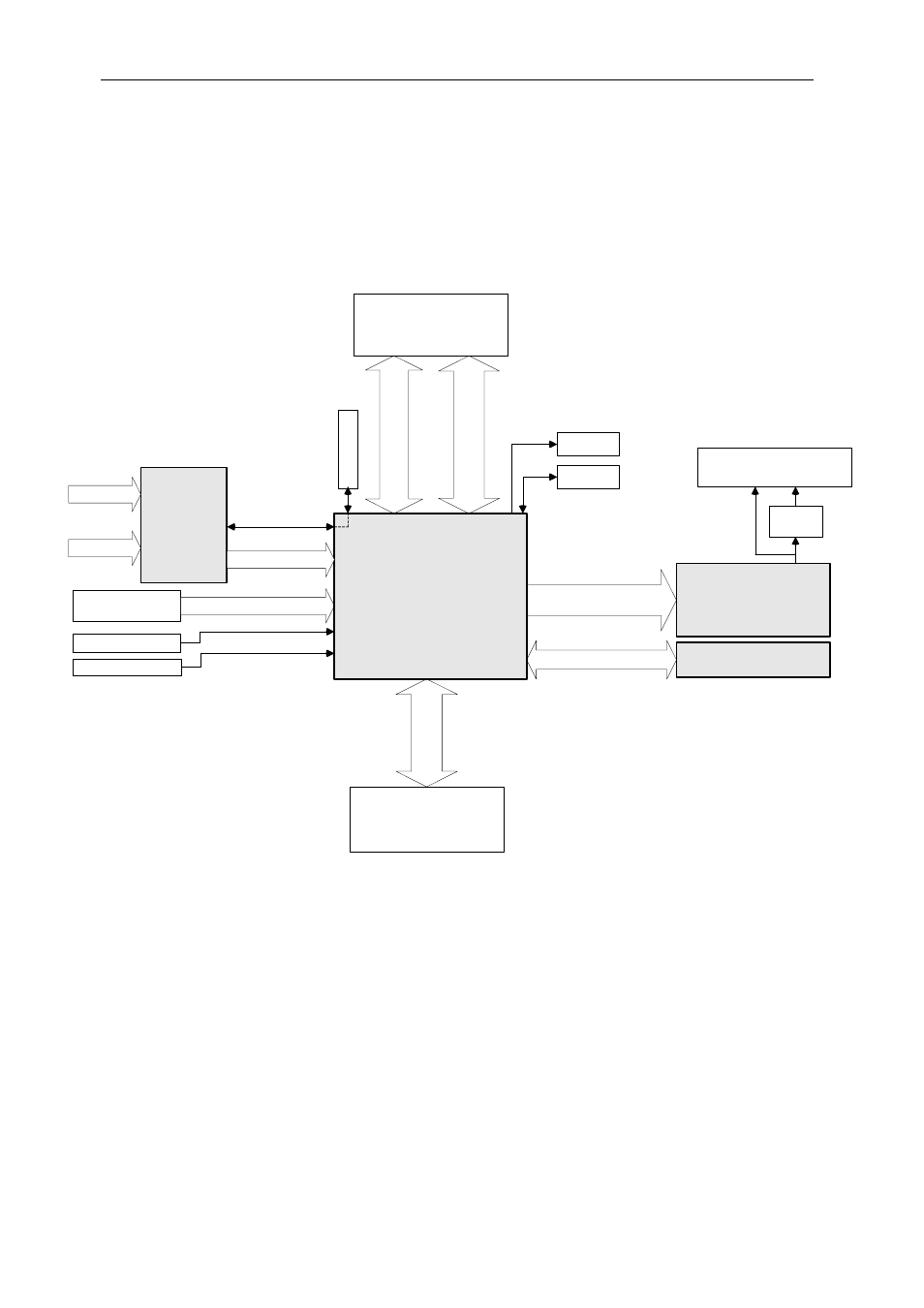
Block Diagram.
The following diagram shows interconnections between main blocks of the SMT377.
Greyed out blocks represent the main devices fitted on the board. Other blocks are
on-board connectors or secondary devices.
Sundance High-speed
Bus (SHB) - input
60 I/O Pins; 32-bit Data
1x
C
ompor
t
12
I/O
pins
Timer,
& Co
n
trol
15
I/O
pins
2x C
om
po
rt
s
24
I/
O pi
ns
47 I/O pins
9 I/O Pins; Serial DATA-Bus
OpAmp
2 x T.I. DAC7634
16-bit @ 100kHz
Digital-to-Analog Converter
48-pins SSOP package
Two banks of ZBT-RAM
memory of 4MBytes each
Xilinx CPLD
XC9636XL
CS48
on Comport #3
and #4
JTA
G
Head
e
r
J1 Top Primary TIM
Connector
Comport 3
J2 Bottum Primary TIM
Connector
Comports 1 and 4
MMBX DAC Headers
0.1" Type
External Trigger
4 LEDs
External DAC Clock
Xilinx FPGA Virtex-II
FG456 -4
324 I/O Pins
1.5V
4 I/O pins
Comport 3
Comport 4
FPGA configuration
Figure 1 - Block diagram.
- SMT107 (16 pages)
- SMT6035 v.2.2 (39 pages)
- SMT6012 v.4.6 (22 pages)
- FC100 (12 pages)
- FC108 v.1.1 (10 pages)
- SMT6065 v.4.0 (45 pages)
- FFT v.2.1 (19 pages)
- SMT111 (18 pages)
- SMT118LT (10 pages)
- SMT118 (20 pages)
- SMT123-SHB (13 pages)
- SMT128 (15 pages)
- SMT145 (18 pages)
- SMT148 (35 pages)
- SMT130 v.1.0 (46 pages)
- SMT148FX (48 pages)
- SMT310Q (55 pages)
- PARS (70 pages)
- SMT166-FMC (52 pages)
- SMT166 (44 pages)
- SMT300Q v.1.6 (61 pages)
- SMT310 v.1.6 (50 pages)
- SMT317 (24 pages)
- SMT326v2 (24 pages)
- SMT338 (19 pages)
- SMT349 (32 pages)
- SMT339 v.1.3 (27 pages)
- SMT338-VP (22 pages)
- SMT358 (25 pages)
- SMT351T (37 pages)
- SMT351 (25 pages)
- SMT350 (45 pages)
- SMT362 (30 pages)
- SMT365G (23 pages)
- SMT364 (37 pages)
- SMT373 (15 pages)
- SMT368 (24 pages)
- SMT370v3 (46 pages)
- SMT381 2007 (31 pages)
- SMT381-VP (81 pages)
- SMT387 (42 pages)
- SMT391 (18 pages)
- SMT384 (47 pages)
- SMT390-VP (55 pages)