Shb a data – Sundance SMT370v2 User Manual
Page 15

Version 2.0
Page 15 of 46
SMT370v2/v3 User Manual
three control signals: write enable, request and acknowledge. An SHB bus can also
be divided into two 16-bit buses and one 8-bit bus.
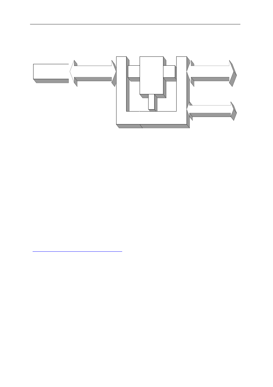
Here is the architecture of the SHB interface implemented into the FPGA:
D[0..31]
FIFO
256 x 32 x 2
D[0..15]
Control Logic and Status
CLK WEN REQ ACK
SHB A
DATA
Figure 4 - SHB interface structure.
Communication links implemented on the SMT370.
The SMT370 provides 2 ComPort links. They are given the numbers 0 and 3. The
default firmware provided with the board implements ComPort3 as a control register
communication port, which means that every control register word has to be sent to
ComPort3 on the SMT370 to be received.
The board also connects two full SHB connectors (60 bits) to the FPGA. The FPGA
implements two 16-bit (or one 32-bit) unidirectional interfaces per SHB connector:
output only for SHBA – used to send out samples coming from both ADCs - and input
only for SHBB – used to suck samples in to the DAC.
For more details about ComPorts and SHB.
The following link will give you more information:
External_Interface_User_manual.pdf
