Serial ports & other c60 i/o, Fpga and cpld jtag, Serial ports & other c60 i/o fpga and cpld jtag – Sundance SMT365G User Manual
Page 18
Version 1.0.0
Page 18 of 23
SMT365G User Manual
Serial Ports & Other C60 I/O
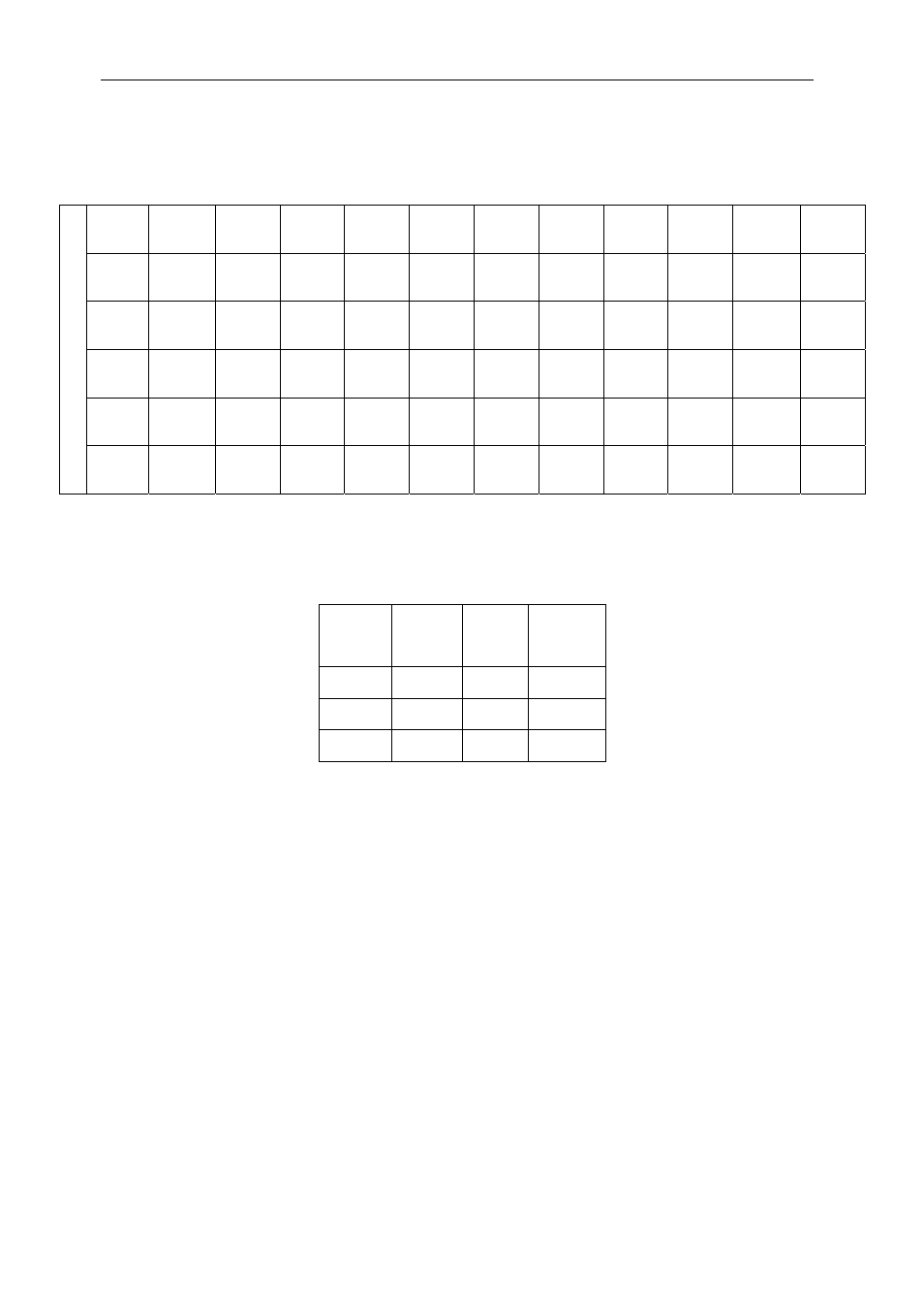
The C60 contains various I/O ports. These signals are connected to a 0.1” pitch DIL
pin header. The pin-out of this connector is shown here:
P
O
TTL1 TTL0 GND GND GPIO7 GPIO6 GPIO5 GPIO4 GPIO3 GPIO2
CLK / 6
GPIO1
CLK / 4
GPIO0
L
A
TTL3 TTL2 V33 V33 GPIO15
GPIO14
GPIO13 GPIO12 GPIO11 GPIO10 GPIO9 NC
R
I
URD0
URD1 URD2 URD3 URD4 URD5 URD6 URD7 URCLK
URENB
URCLAV
URSOC
S
A
UXD0
UXD1 UXD2 UXD3 UXD4 UXD5 UXD6 UXD7 UXCLK
UXENB
UXCLAV
UXSOC
T
I
UXA0 DR1
UXA1
FSR1
UXA2
FSX1
UXA3
DX1
UXA4
CLKS2
GPIO8
CLKX2 CLKR2 FSX2 DX2
FSR2 DR2
O
N
URA0 URA1 CLKR1
URA2
CLKX1
URA4
CLKS1
URA3
CLKS0 CLKX0 CLKR0 FSX0 DX0
FSR0 DR0
FPGA and CPLD JTAG
The following shows the pin-outs for JP2 (CPLD) and JP3 (FPGA) JTAG connectors:
Signal Pin Pin Signal
V33 1 2 TMS
TCK 3 4 TDO
GND 5 6 TDI