Sundance SMT358 User Manual
Page 9

Version 2.5
Page 9 of 25
SMT358 User Manual
Figure 1 shows the block diagram of the SMT358 I/O module. The following section
describes the SMT358 from a user’s point of view. Reference is made to the different blocks
of Figure 1 in the next Figures.
On-board SRAM
The SMT358 provides the user with pipelined or Flowthrough ZBT (Zero Bus Turnaround)
SRAM from Micron. Therefore this type of SRAM is optimised for a 100 percent bus
utilisation eliminating any cycle when transitioning from READ to WRITE or vice versa.
Three Chip Enables allow easy depth expansion so that the SMT358 total amount of memory
can vary from 4 MBytes up to 16 MBytes.
Micron 4,8 or 16 Mbit ZBTSRAM have compatible inputs and outputs. FPGA designers can
find the general description and a Pin description in the latest data sheets on Micron’s Web
Site at
http://www.micron.com/mti/msp/html/zbtds.html
The on-board memory is divided into four banks (bank 1 to 4) accessible on a 72-bit bus (4
18-bit busses) and can be run at frequencies up to 166Mhz and.
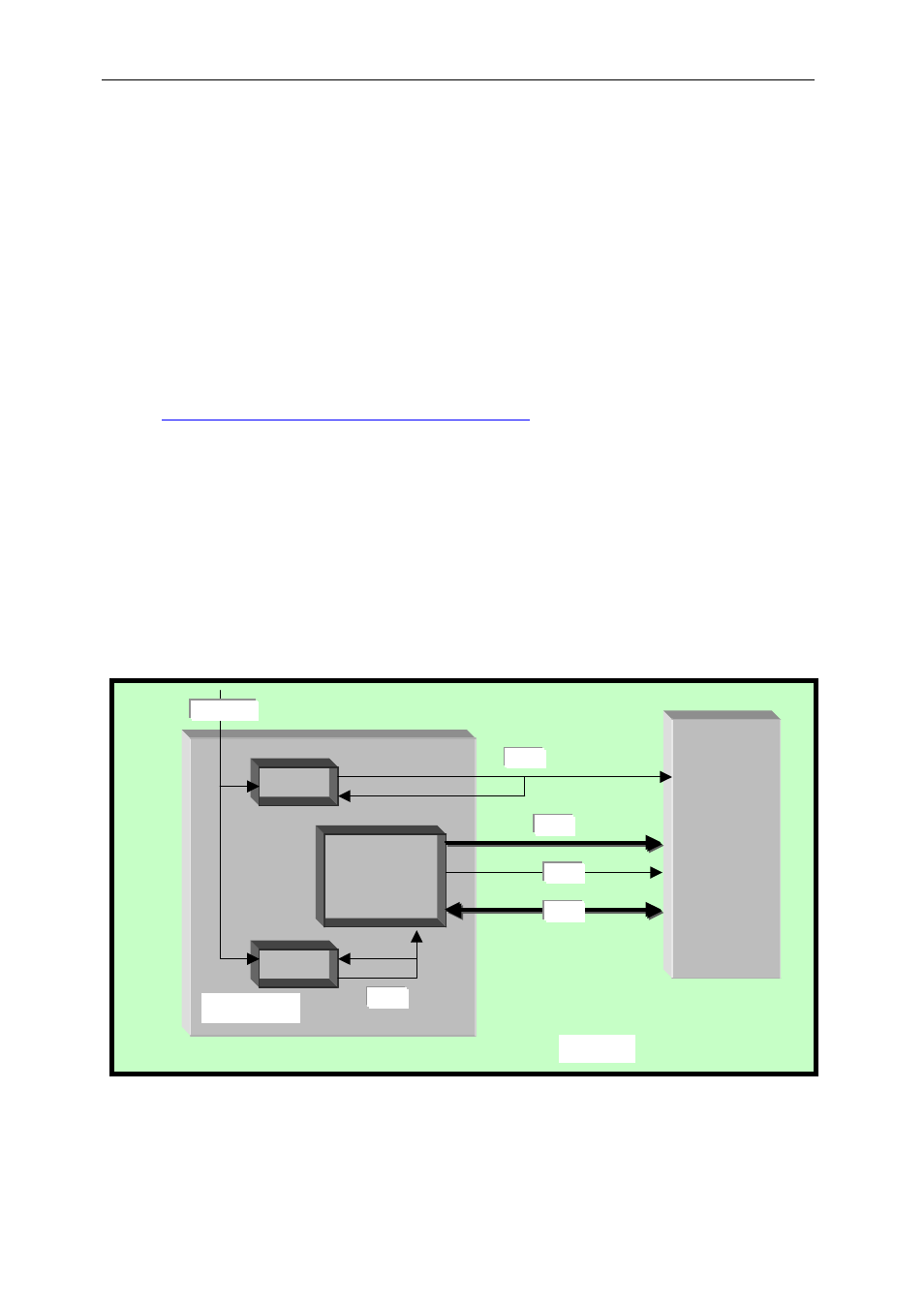
Each of the 4 SRAM banks is independently accessible (Control, Data and Address are
independent for every bank) and share the same Clock signal. To ensure high performance,
the clock signal can be de-skewed inside the FPGA using DLLs as reproduced in Figure 2. As
a result, a high-speed de-skewed clock drives the controller inside the FPGA and the ZBT
SRAM.
The Virtex provides four programmable DLLs to produce waveforms with a wide range of
frequencies and duty cycles.
Figure 2: ZBT SRAM Clock signal
Z
B
T
S
R
A
M
BA
N
K
1, 2,3,4
CONTROLLER
DLL
DLL
BoardClk
Clk2x
Clk2x
Addr
Data
RNW
VIRTEX/E
SMT358
