Sensoray 421 User Manual
Page 17
Sensoray Model 421 Instruction Manual
Page 15
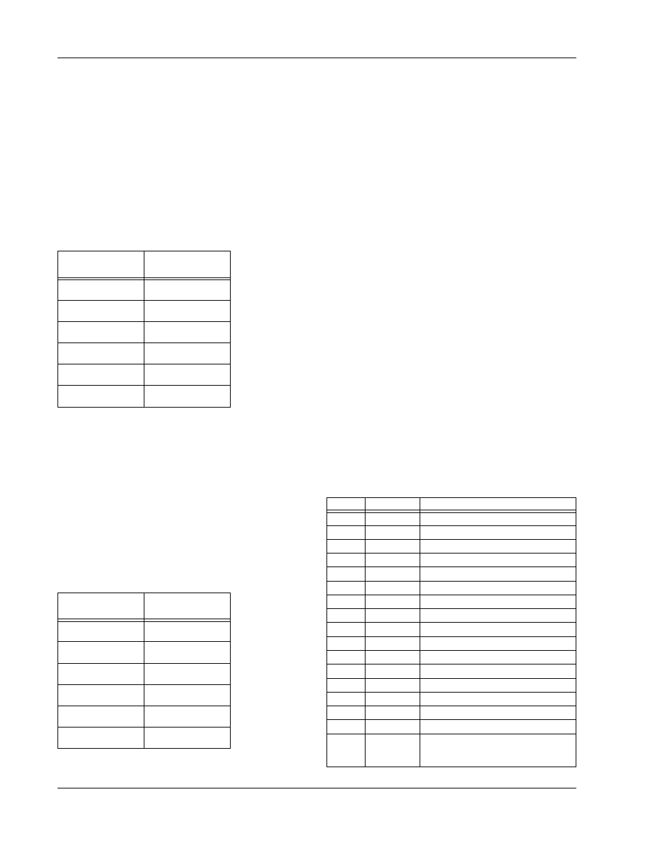
Unipolar-mode Transfer Function
As discussed earlier, A/D output codes are
represented as 12-bit unsigned integers in the
unipolar mode. Output values range from 0 at zero
volts input to 4095 at the positive full-scale input
voltage.
The following table shows the relationship between
input voltage and A/D output codes. A 0 to +10 volt
gain range (unity gain) is assumed for this
illustration.
Input Voltage
Output Code
0.000V
000
2.441mV
001
4.998V
7FF
5.000V
800
5.002V
801
+9.997V
FFF
Bipolar-mode Transfer Function
A/D output codes are formatted as 12-bit signed
two’s complement integers in the bipolar mode.
Output values range from -2048 at negative full-scale
input to +2047 at positive full-scale input voltage.
The following table shows the relationship between
input voltage and A/D output codes. A -5 to +5 volt
gain range (unity gain) is assumed for this
illustration.
Input Voltage
Output Code
-5.000V
800
-4.997V
801
-2.441mV
FFF
0.000V
000
+2.441mV
001
+4.997V
7FF
Input Connections
Each analog input channel makes two connections to
the 421 board. These two connections constitute a
differential input pair. The digitizer measures the
difference in voltage between the two inputs.
Note that the input common-mode voltage — the
voltage at either input relative to ISAbus five volt
return (GND) — should not exceed plus or minus 10
volts. Minor excursions beyond this limit will cause
inaccurate measurements. Significant excursions
may result in damage to digitizer circuitry. Refer to
the 421 specifications section for further details.
All analog input sources should be referenced to
ISAbus GND. If you are connecting an isolated
source (a source not referenced to GND), you should
tie one side of the source to GND. Since analog input
channels are true differential, it doesn’t matter which
side is connected to GND.
Connector Pinout
All differential analog inputs connect to 40-pin
header connector P2. This connector is shared by 421
analog input and analog output functions. The table
below describes that portion of P2 related to analog
input functions. Note that the GND signals are
related to both analog input and output functions.
Connector P2: Analog I/O
Pin
Name
Function
2
ADC0+
A/D channel 0 positive input
4
ADC0-
A/D channel 0 negative input
6
ADC1+
A/D channel 1 positive input
8
ADC1-
A/D channel 1 negative input
10
ADC2+
A/D channel 2 positive input
12
ADC2-
A/D channel 2 negative input
14
ADC3+
A/D channel 3 positive input
16
ADC3-
A/D channel 3 negative input
18
ADC4+
A/D channel 4 positive input
20
ADC4-
A/D channel 4 negative input
22
ADC5+
A/D channel 5 positive input
24
ADC5-
A/D channel 5 negative input
26
ADC6+
A/D channel 6 positive input
28
ADC6-
A/D channel 6 negative input
30
ADC7+
A/D channel 7 positive input
32
ADC7-
A/D channel 7 negative input
33,34,
38,39,
40
GND
Analog common