Measurement Computing PPIO-AI08 User Manual
Page 13
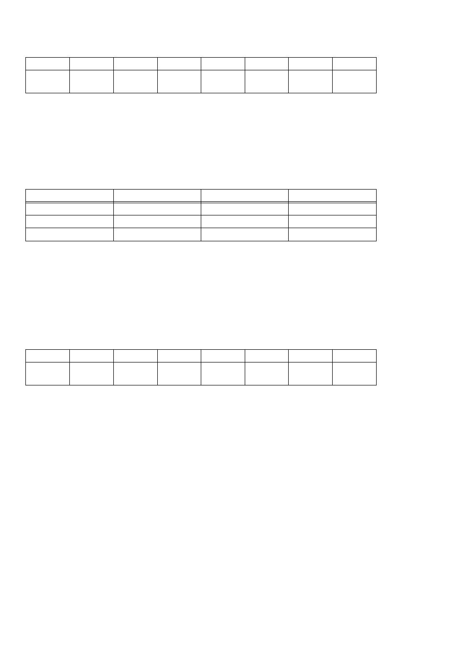
5.3.1 A/D Data Registers
BASE + 0
A/D8
A/D7
A/D6
A/D5
A/D4
A/D3
A/D2
A/D1
MSB
0
1
2
3
4
5
6
7
READ
On read, the most significant A/D byte is read. Note that since data is read through
the parallel port four bits at a time, two reads are required to obtain the entire byte
from this register.
The table below has coding for input voltages.
0 volts
−Full Scale
0
0
½ Full Scale
0 Volts
800
2048
y
Full Scale
y
Full Scale
FFF
4095
UNIPOLAR
BIPOLAR
HEX
DECIMAL
WRITE
Writing to this register starts a 12-bit A/D conversion.
A note of caution:
Place a program loop of at least 25
µ
s delay between consecutive 12
bit A/D conversions to avoid over-running the A/D converter.
BASE + 1
0
0
0
0
A/D12
LSB
A/D11
A/D10
A/D9
0
1
2
3
4
5
6
7
A read/write register.
READ
On read, it contains the least significant four digits of the Analog input data.
These four bits of analog input data must be combined with the eight bits of analog
input data in
BASE
+ 0, forming a complete 12 bit number. The data is in the formof
0 = minus full scale. 4095 = +FS.
WRITE
Writing any data to the register causes an immediate 8-bit A/D conversion.
9